
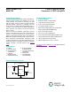
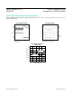
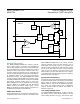
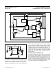
Datasheet

OUT, SHDN, BATT, LX to GND ...............................-0.3V to +6V
FB to GND .............................................. -0.3V to (V
OUT
+ 0.3V)
OUT, LX Current ......................................................................1A
Continuous Power Dissipation (T
A
= +70°C)
5-Pin Thin SOT (derate 2.7mW/°C above +70°C) ...219.10mW
Operating Temperature Range ........................... -40°C to +85°C
Junction Temperature ...................................................... +150°C
Storage Temperature Range ............................ -65°C to +150°C
Soldering Temperature
Lead(Pb)-free packages ..............................................+260°C
Packages containing lead(Pb) .....................................+240°C
(V
BATT
= 1.2V, V
OUT
= 3.3V (MAX1722/MAX1723), V
OUT
= V
OUT(NOM)
(MAX1724), SHDN = OUT, R
L
= ∞, T
A
= 0°C to +85°C,
unless otherwise noted. Typical values are at T
A
= +25°C.) (Note 1)
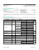
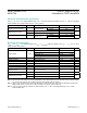
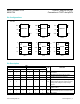
PARAMETER SYMBOL CONDITIONS MIN TYP MAX UNITS
Minimum Input Voltage MAX1722/MAX1724 0.8 V
Operating Input Voltage V
IN
T
A
= +25°C
MAX1722/MAX1724 0.91 5.5
V
MAX1723 (Note 2) 1.2 5.5
Minimum Start-Up Input Voltage
T
A
= +25°C,
R
L
= 3kΩ
MAX1722/MAX1724 0.83 0.91
V
MAX1723 (Note 2) 0.87 1.2
Output Voltage V
OUT
MAX1724E__27
T
A
= +25°C 2.673 2.7 2.727
V
T
A
= 0°C to +85°C 2.633 2.767
MAX1724E__30
T
A
= +25°C 2.970 3.0 3.030
T
A
= 0°C to +85°C 2.925 3.075
MAX1724E__33
T
A
= +25°C 3.267 3.3 3.333
T
A
= 0°C to +85°C 3.218 3.383
MAX1724E__50
T
A
= +25°C 4.950 5.0 5.050
T
A
= 0°C to +85°C 4.875 5.125
Output Voltage Range V
OUT
MAX1722/MAX1723 2 5.5 V
Feedback Voltage V
FB
MAX1722/MAX1723
T
A
= +25°C 1.223 1.235 1.247
V
T
A
= 0°C to +85°C 1.210 1.260
Feedback Bias Current I
FB
MAX1722/MAX1723
T
A
= +25°C 1.5 20
nA
T
A
= +85°C 2.2
N-Channel On-Resistance R
DS(ON)
V
OUT
forced to 3.3V 0.5 1.0 Ω
P-Channel On-Resistance R
DS(ON)
V
OUT
forced to 3.3V 1.0 2.0 Ω
N-Channel Switch Current Limit I
LIM
V
OUT
forced to 3.3V 400 500 600 mA
Switch Maximum On-Time t
ON
3.5 5 6.5 µs
Synchronous Rectier Zero-
Crossing Current
V
OUT
forced to 3.3V 5 20 35 mA
Quiescent Current into OUT (Notes 3, 4) 1.5 3.6 µA
Shutdown Current into OUT
MAX1723/MAX1724
(Notes 3, 4)
T
A
= +25°C 0.01 0.5
µA
T
A
= +85°C 0.1
Quiescent Current into BATT
MAX1722/MAX1724
(Note 4)
T
A
= +25°C 0.001 0.5
µA
T
A
= +85°C 0.01
MAX1722/MAX1723/
MAX1724
1.5μA I
Q
, Step-Up DC-DC
Converters in TSOT and µDFN
www.maximintegrated.com
Maxim Integrated
│
2
Absolute Maximum Ratings
Stresses beyond those listed under “Absolute Maximum Ratings” may cause permanent damage to the device. These are stress ratings only, and functional operation of the device at these
or any other conditions beyond those indicated in the operational sections of the specifications is not implied. Exposure to absolute maximum rating conditions for extended periods may affect
device reliability.
Electrical Characteristics