
Datasheet

BATT/Damping Switch
(MAX1722/MAX1724)
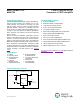
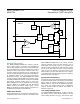
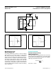
The MAX1722/MAX1724 include an internal damping
switch (Figure 4) to minimize ringing at LX and reduce
EMI. When the energy in the inductor is insufficient to
supply current to the output, the capacitance and induc-
tance at LX form a resonant circuit that causes ringing.
The damping switch supplies a path to quickly dissipate
this energy, suppressing the ringing at LX. This does
not reduce the output ripple, but does reduce EMI with
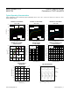
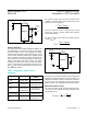
minimal impact on efficiency. Figures 5 and 6 show the
LX node voltage waveform without and with the damping
switch, respectively.
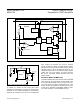
Design Procedure
Setting the Output Voltage
(MAX1722/MAX1723)
The output voltage can be adjusted from 2V to 5.5V using
external resistors R1 and R2 (Figure 7). Since FB leakage
is 20nA (max), select feedback resistor R1 in the 100kΩ to
1MΩ range. Calculate R2 as follows:
OUT
FB
V
R 2 R1 1
V
= −
where V
FB
= 1.235V.
Figure 4. Simplified Diagram of Damping Switch
Figure 5. LX Ringing Without Damping Switch (MAX1723)
Figure 6. LX Ringing With Damping Switch (MAX1722/MAX1724)
MAX1722
MAX1724
PDRV
DAMP
NDRV
TIMING
CIRCUIT
OUT
V
OUT
V
IN
BATT
LX
DAMPING
SWITCH
GND
P
N
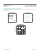
1µs/div
1V/div
1µs/div
1V/div
MAX1722/MAX1723/
MAX1724
1.5μA I
Q
, Step-Up DC-DC
Converters in TSOT and µDFN
www.maximintegrated.com
Maxim Integrated
│
9