
Datasheet
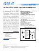


MAX17600–MAX17605
4A Sink /Source Current, 12ns, Dual MOSFET Drivers
2
V
DD
, INA, INB, ENA, ENB to GND ........................ -0.3V to +16V
OUTA, OUTB to GND ............................................-0.3V to +16V
Junction Operating Temperature Range ......... -40NC to +125NC
Continuous Power Dissipation (T
A
= +70NC)
8-Pin TDFN (derate 23.8mW/NC above +70NC) ........1904mW
8-Pin SO (derate 74mW/NC above +70NC) ............. 588.2mW*
8-Pin FMAX (derate 12.9mW/NC above +70NC) .....1030.9mW
Operating Temperature Range ........................ -40NC to +125NC
Junction Temperature ................................................... +150NC
Storage Temperature Range ............................ -65NC to +150NC
Lead Temperature (soldering, 10s) ................................+300NC
Soldering Temperature (reflow) ......................................+240NC
*As per JEDEC 51 standard.
TDFN
Junction-to-Ambient Thermal Resistance (B
JA
) ..........42NC/W
Junction-to-Case Thermal Resistance (B
JC
) .................8NC/W
SO
Junction-to-Ambient Thermal Resistance (B
JA
) ........136NC/W
Junction-to-Case Thermal Resistance (B
JC
) ...............38NC/W
FMAX
Junction-to-Ambient Thermal Resistance (B
JA
) .......77.6NC/W
Junction-to-Case Thermal Resistance (B
JC
) .................5NC/W
ABSOLUTE MAXIMUM RATINGS
Note 1: Package thermal resistances were obtained using the method described in JEDEC specification JESD51-7, using a four-
layer board. For detailed information on package thermal considerations, refer to www.maxim-ic.com/thermal-tutorial.
Stresses beyond those listed under “Absolute Maximum Ratings” may cause permanent damage to the device. These are stress ratings only, and functional opera-
tion of the device at these or any other conditions beyond those indicated in the operational sections of the specifications is not implied. Exposure to absolute
maximum rating conditions for extended periods may affect device reliability.
PACKAGE THERMAL CHARACTERISTICS (Note 1)
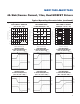
ELECTRICAL CHARACTERISTICS
(V
DD
= 12V, C
L
= 0F, at T
A
= -40NC to +125NC, unless otherwise noted. Typical values are specified at T
A
= +25NC. Parameters
specified at V
DD
= 4V apply to the TTL versions only.) (Note 2)
PARAMETER SYMBOL CONDITIONS MIN TYP MAX UNITS
POWER SUPPLY (V
DD
)
V
DD
Operating Range V
DD
TTL versions 4 14
V
HNM versions 6 14
V
DD
Undervoltage Lockout UVLO V
DD
rising 3 3.5 3.85 V
V
DD
UVLO Hysteresis 200 mV
V
DD
UVLO to OUT_ Delay V
DD
rising 120
Fs
V
DD
Supply Current
IDD_Q Not switching, V
DD
= 14V (Note 3) 1 2
mA
IDD_SW
V
DD
= 4.5V, C
L
= 1nF, both channels
switching at 1MHz
12 18
DRIVER OUTPUT (SOURCE) (OUTA, OUTB)
Peak Output Current (Sourcing) I
PK-P
V
DD
= 14V, C
L
= 10nF (Note 3) 4 A
Driver Output Resistance Pulling Up
(Note 4)
R
ON-P
V
DD
= 14V, I
OUT_
= 100mA 0.88 1.85
I
V
DD
= 4V, I
OUT_
= 100mA 0.91 1.95
DRIVER OUTPUT (SINK) (OUTA, OUTB)
Peak Output Current (Sinking) I
PK-N
V
DD
= 14V, C
L
= 10nF (Note 3) 4 A
Driver Output Resistance Pulling
Down (Note 4)
R
ON-N
V
DD
= 14V, I
OUT_
= -100mA 0.5 0.95
I
V
DD
= 4V, I
OUT_
= -100mA 0.52 1