
Datasheet


MAX17600–MAX17605
4A Sink /Source Current, 12ns, Dual MOSFET Drivers
1
General Description
The MAX17600–MAX17605 devices are high-speed
MOSFET drivers capable of sinking /sourcing 4A peak
currents. The devices have various inverting and non-
inverting part options that provide greater flexibility in
controlling the MOSFET. The devices have internal logic
circuitry that prevents shoot-through during output-state
changes. The logic inputs are protected against voltage
spikes up to +14V, regardless of V
DD
voltage. Propagation
delay time is minimized and matched between the dual
channels. The devices have very fast switching time,
combined with short propagation delays (12ns typ),
making them ideal for high-frequency circuits. The
devices
operate from a +4V to +14V single power
supply and typically consume 1mA of supply cur-
rent. The MAX17600/MAX17601 have standard TTL
input logic levels, while the MAX17603/MAX17604/
MAX17605 have CMOS-like high-noise margin (HNM)
input logic levels. The MAX17600/MAX17603 are dual
inverting input drivers, the MAX17601/MAX17604 are
dual noninverting input drivers, and the MAX17602 /
MAX17605 devices have one noninverting and one
inverting input. These devices are provided with enable
pins (ENA, ENB) for better control of driver operation.
These devices are available in 8-pin (3mm x 3mm) TDFN,
8-pin (3mm x 5mm) FMAX
®
, and 8-pin SO packages and
operate over the -40NC to +125NC temperature range.
Applications
Power MOSFET Switching
Switch-Mode Power Supplies
DC-DC Converters
Motor Control
Power-Supply Modules
Features
S Dual Drivers with Enable Inputs
S +4V to +14V Single Power-Supply Range
S 4A Peak Sink /Source Current
S Inputs Rated to +14V, Regardless of V
DD
Voltage
S Low 12ns Propagation Delay
S 6ns Typical Rise and 5ns Typical Fall Times with
1nF Load
S Matched Delays Between Channels
S Parallel Operation of Dual Outputs for Larger
Driver Output Current
S TTL or HNM Logic-Level Inputs with Hysteresis for
Noise Immunity
S Low Input Capacitance: 10pF (typ)
S Thermal Shutdown Protection
S TDFN, µMAX, and SO Package Options
S -40NC to +125NC Operating Temperature Range
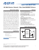
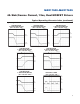
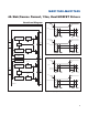
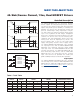
Typical Operating Circuit
19-6177; Rev 1; 5/12
Ordering Information appears at end of data sheet.
µMAX is a registered trademark of Maxim Integrated
Products, Inc.
EVALUATION KIT AVAILABLE
GND
OUTB
ENB
OUTA
ENA
V
DD
V
DD
(UP TO +14V)
INA
INB
MAX17600
MAX17601
MAX17602
MAX17603
MAX17604
MAX17605
For pricing, delivery, and ordering information, please contact Maxim Direct
at 1-888-629-4642, or visit Maxim’s website at www.maxim-ic.com.