
Datasheet
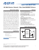


MAX17600–MAX17605
4A Sink /Source Current, 12ns, Dual MOSFET Drivers
10
Undervoltage Lockout (UVLO)
When V
DD
is below the UVLO threshold, the output
stage n-channel device is on and the p-channel is off,
independent of the state of the inputs. This holds the
outputs low. The UVLO is typically 3.6V with 200mV
typical hysteresis to avoid chattering. A typical falling
delay of 2Fs makes the UVLO immune to narrow negative
transients in noisy environments.
Driver Outputs
The devices feature 4A peak sourcing/sinking capa-
bilities to provide fast rise and fall times of the MOSFET
gate. Add a resistor in series with OUT_ to slow the cor-
responding rise/fall time of the MOSFET gate.
Applications Information
Supply Bypassing, Device
Grounding, and Placement
Ample supply bypassing and device grounding are
extremely important because when large external
capacitive loads are driven, the peak current at the V
DD
pin can approach 4A, while at the GND pin, the peak
current can approach 4A. V
DD
drops and ground shifts
are forms of negative feedback for inverters and, if
excessive, can cause multiple switching when the
inverting input is used and the input slew rate is low. The
device driving the input should be referenced to the devic-
es’ GND pin, especially when the inverting input is used.
Ground shifts due to insufficient device grounding can
disturb other circuits sharing the same AC ground return
path. Any series inductance in the V
DD
, OUT_, and/or
GND paths can cause oscillations due to the very high
di/dt that results when the devices are switched with any
capacitive load. A 2.2FF or larger value ceramic
capacitor is recommended, bypassing V
DD
to GND and
placed as close as possible to the pins. When driving
very large loads (e.g., 10nF) at minimum rise time, 10FF or
more of parallel storage capacitance is recommended. A
ground plane is highly recommended to minimize ground
return resistance and series inductance. Care should be
taken to place the devices as close as possible to the
external MOSFET being driven to further minimize board
inductance and AC path resistance.
Power Dissipation
Power dissipation of the devices consists of three
components, caused by the quiescent current, capacitive
charge and discharge of internal nodes, and the output
current (either capacitive or resistive load). The sum of
these components must be kept below the maximum
power-dissipation limit.
The quiescent current is 1mA typical. The current
required to charge and discharge the internal nodes
is frequency dependent (see the Typical Operating
Characteristics). The devices’ power dissipation when
driving a ground referenced resistive load is:
P = D x R
ON
(MAX) x I
LOAD
2 per channel
where D is the fraction of the period the devices’ output
pulls high, R
ON
(MAX) is the maximum pullup on-resist-
ance of the device with the output high, and I
LOAD
is the
output load current of the devices.
For capacitive loads, the power dissipation is:
P = C
LOAD
x (V
DD
)
2
x FREQ per channel
where C
LOAD
is the capacitive load, V
DD
is the supply
voltage, and FREQ is the switching frequency.
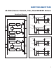
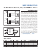
Layout Information
The devices’ MOSFET drivers source and sink large
currents to create very fast rise and fall edges at the
gate of the switching MOSFET. The high di/dt can cause
unacceptable ringing if the trace lengths and
impedances are not well controlled. The following PCB
layout guidelines are recommended when designing with
the devices:
• Placeatleastone2.2FF decoupling ceramic capacitor
from V
DD
to GND as close as possible to the IC. At least
one storage capacitor of 10FF (min) should be located
on the PCB with a low-resistance path to the V
DD
pin
of the devices. There are two AC current loops formed
between the IC and the gate of the MOSFET being
driven. The MOSFET looks like a large capacitance
from gate to source when the gate is being pulled low.
The active current loop is from OUT_ of the devices to
the MOSFET gate to the MOSFET source and to GND
of the devices. When the gate of the MOSFET is being
pulled high, the active current loop is from OUT_ of the
devices to the MOSFET gate to the MOSFET source to
the GND terminal of the decoupling capacitor to the
V
DD
terminal of the decoupling capacitor and to the
V
DD
terminal of the devices. While the charging current
loop is important, the discharging current loop is also
critical. It is important to minimize the physical distance
and the impedance in these AC current paths.
• In a multilayer PCB, the component surface layer
surrounding the devices should consist of a ground plane
containing the discharging and charging current loops.