
Datasheet


MAX17600–MAX17605
4A Sink /Source Current, 12ns, Dual MOSFET Drivers
11
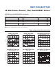
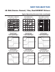
Ordering Information/Selector Guide
Note: All devices are specified over the -40°C to +125°C temperature range. Optional 8-pin 2mm x 3mm TDFN package is
available. Contact your Maxim sales representative for more information.
+Denotes a lead(Pb)-free/RoHS-compliant package.
*EP = Exposed pad.
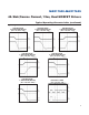
Package Information
For the latest package outline information and land patterns
(footprints), go to www.maxim-ic.com/packages. Note that a
“+”, “#”, or “-” in the package code indicates RoHS status only.
Package drawings may show a different suffix character, but
the drawing pertains to the package regardless of RoHS status.
Chip Information
PROCESS: BiCMOS
PART PIN-PACKAGE CONFIGURATION LOGIC LEVELS TOP MARK
MAX17600ATA+ 8 TDFN-EP* (3mm x 3mm) Dual/Inverting TTL +BOJ
MAX17600ASA+ 8 SO Dual/Inverting TTL +
MAX17600AUA+
8 FMAX-EP*
Dual/Inverting TTL +AACI
MAX17601ATA+ 8 TDFN-EP* (3mm x 3mm) Dual/Noninverting TTL +BOK
MAX17601ASA+ 8 SO Dual/Noninverting TTL +
MAX17601AUA+
8 FMAX-EP*
Dual/Noninverting TTL +AACJ
MAX17602ATA+ 8 TDFN-EP* (3mm x 3mm) Inverting/Noninverting TTL +BOL
MAX17602ASA+ 8 SO Inverting/Noninverting TTL +
MAX17602AUA+
8 FMAX-EP*
Inverting/Noninverting TTL +AACK
MAX17603ATA+ 8 TDFN-EP* (3mm x 3mm) Dual/Inverting HNM +BOM
MAX17603ASA+ 8 SO Dual/Inverting HNM +
MAX17603AUA+
8 FMAX-EP*
Dual/Inverting HNM +AACL
MAX17604ATA+ 8 TDFN-EP* (3mm x 3mm) Dual/Noninverting HNM +BON
MAX17604ASA+ 8 SO Dual/Noninverting HNM +
MAX17604AUA+
8 FMAX-EP*
Dual/Noninverting HNM +AACM
MAX17605ATA+ 8 TDFN-EP* (3mm x 3mm) Inverting/Noninverting HNM +BOO
MAX17605ASA+ 8 SO Inverting/Noninverting HNM +
MAX17605AUA+
8 FMAX-EP*
Inverting/Noninverting HNM +AACN
PACKAGE
TYPE
PACKAGE
CODE
OUTLINE
NO.
LAND
PATTERN NO.
8 TDFN-EP T833+2
21-0137 90-0059
8 SO S8+2
21-0041 90-0096
8 FMAX
U8E+2
21-0107 90-0145