
Datasheet


MAX17600–MAX17605
4A Sink /Source Current, 12ns, Dual MOSFET Drivers
7
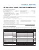
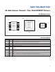
Pin Description
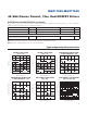
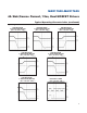
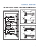
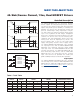
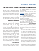
Pin Configurations
PIN NAME FUNCTION
1 ENA
Enable Input for Driver A. Internally pulled to V
DD
through a 100kI resistor. Leave unconnected for
always-on operation. Connect to GND for disabling the corresponding channel.
2 INA Logic Input for Channel A
3 GND Ground
4 INB Logic Input for Channel B
5 OUTB
Channel B Driver Output. Sources and sinks current for channel B to turn the external MOSFET at OUTB
on or off.
6 V
DD
Power-Supply Input. Bypass to GND with one or more low-ESR 0.1FF ceramic capacitors.
7 OUTA
Channel A Driver Output. Sources and sinks current for channel A to turn the external MOSFET at OUTA
on or off.
8 ENB
Enable Input for Driver B. Internally pulled to V
DD
through a 100kI resistor. Leave unconnected for
always-on operation. Connect to GND for disabling the corresponding channel.
— EP Exposed Pad (TDFN Only). Internally connected to GND. Do not use the EP as the only ground connection.
ENA
+
INA
GND
1
2
3
4
8
7
6
5INB
ENB
OUTA
V
DD
OUTB
SO
TOP VIEW
MAX17600
MAX17601
MAX17602
MAX17603
MAX17604
MAX17605
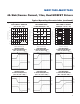
134
+
865
ENB V
DD
OUTB
2
7
OUTA
ENA GND INBINA
TDFN
TOP VIEW
MAX17600
MAX17601
MAX17602
MAX17603
MAX17604
MAX17605
TOP VIEW
1
2
3
4
8
7
6
5
ENB
OUTA
V
DD
OUTBINB
GND
INA
ENA
µMAX
+
MAX17600
MAX17601
MAX17602
MAX17603
MAX17604
MAX17605