
Datasheet


+1.2V to +5.5V, ±15kV ESD-Protected, 0.1µA,
35Mbps, 8-Channel Level Translators
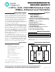
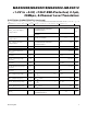
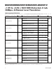
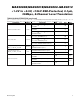
Pin Description
PIN
TSSOP
UCSP TQFN
NAME FUNCTION
1 B1 19 I/O V
L
1 Input/Output 1, Referenced to V
L
2A120 V
L
Logic Input Voltage, +1.2V ≤ V
L
≤ V
CC
. Bypass V
L
to GND with a 0.1µF capacitor.
3 A2 1 I/O V
L
2 Input/Output 2, Referenced to V
L
4 B2 2 I/O V
L
3 Input/Output 3, Referenced to V
L
5 A3 3 I/O V
L
4 Input/Output 4, Referenced to V
L
6 B3 4 I/O V
L
5 Input/Output 5, Referenced to V
L
7 A4 5 I/O V
L
6 Input/Output 6, Referenced to V
L
8 B4 6 I/O V
L
7 Input/Output 7, Referenced to V
L
9 A5 7 I/O V
L
8 Input/Output 8, Referenced to V
L
10 B5 8 EN
Enable Input. If EN is pulled low, I/O V
CC
1 to I/O V
CC
8 are in three-state, while I/O V
L
1
to I/O V
L
8 have internal 6kΩ pulldown resistors. Drive EN high (V
L
) for normal
operation.
11 C5 9 GND Ground
12 D5 10
I/O V
CC
8
Input/Output 8, Referenced to V
CC
13 C4 11
I/O V
CC
7
Input/Output 7, Referenced to V
CC
14 D4 12
I/O V
CC
6
Input/Output 6, Referenced to V
CC
15 C3 13
I/O V
CC
5
Input/Output 5, Referenced to V
CC
16 D3 14
I/O V
CC
4
Input/Output 4, Referenced to V
CC
17 C2 15
I/O V
CC
3
Input/Output 3, Referenced to V
CC
18 D2 16
I/O V
CC
2
Input/Output 2, Referenced to V
CC
19 D1 17 V
CC
V
CC
Input Voltage, +1.65V ≤ V
CC
≤ +5.5V. Bypass V
CC
to GND with a 0.1µF capacitor.
20 C1 18
I/O V
CC
1
Input/Output 1, Referenced to V
CC
— — EP EP Exposed Pad. Connect to GND.
MAX3000E/MAX3001E/MAX3002
MAX3000E/MAX3001E/MAX3002–MAX3012
10
Maxim Integrated