
Datasheet

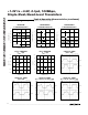

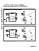
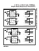

MAX13013/MAX13014/MAX3023
+1.2V to +3.6V, 0.1µA, 100Mbps,
Single-/Dual-/Quad-Level Translators
10 ______________________________________________________________________________________
Detailed Description
The MAX13013/MAX13014/MAX3023 logic-level trans-
lators provide the level shifting necessary to allow
100Mbps data transfer in a multivoltage system.
Externally applied voltages, V
CC
and V
L
, set the logic
levels on either side of the device. Logic signals pre-
sent on the V
L
side of the device appear as a higher-
voltage logic signal on the V
CC
side of the device, and
vice-versa. The MAX13013/MAX13014/MAX3023 bidi-
rectional level translators allow data translation in either
direction (V
L
↔V
CC
) on any single data line. The
MAX13013/MAX13014/MAX3023 accept V
L
from +1.2V
to (V
CC
- 0.4V) and operate with V
CC
from +1.65V to
+3.6V, making them ideal for data transfer between
low-voltage ASICs/PLDs and higher voltage systems.
When in tri-state mode, the MAX13013/MAX13014/
MAX3023 reduce the V
CC
supply current to 0.03µA,
and the V
L
supply current to 0.1µA. These devices
operate at a guaranteed data rate of 100Mbps for V
L
>
1.8V.
Level Translation
For proper operation, ensure that +1.65V ≤ V
CC
≤ +3.6V,
and +1.2V ≤ V
L
≤ V
CC
- 0.4V. During power-up
sequencing, V
L
≥ V
CC
does not damage the device.
During power-supply sequencing, when V
CC
is floating
and V
L
is powering up, up to 40mA current can be
sourced to each load on the V
L
side, without the device
latching up. The maximum data rate depends heavily on
the load capacitance (see the Typical Operating
Characteristics Rise/Fall Time graph), output impedance
of the driver, and the operating voltage range (Table 1).
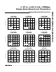
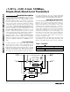
Input Driver Requirements
The MAX13013/MAX13014/MAX3023 architecture is
based on a one-shot accelerator output stage (see
Figure 5). Accelerator output stages are in tri-state
mode except when there is a transition on any of the
translators on the input side, either I/O V
L_
or I/O V
CC_
.
A short pulse is then generated during which the accel-
erator output stages become active and charge/dis-
charge the capacitances at the I/Os. Due to the
architecture, both sides become active during the one-
shot pulse. This can lead to some current feeding into
the external source that is driving the translator.
However, this behavior simply helps to speed up the
transition on the driven side.
For proper operation, the driver has to meet the follow-
ing conditions: less than 25Ω output impedance and
greater than 20mA peak output current capability.
Table 1. Data Rate
V
L
(V) GUARANTEED DATA RATE (Mbps)
V
L
< 1.8 80
V
L
≥ 1.8 100
P
ONE-SHOT
V
CC
V
L
I/O V
L
I/O V
CC
150Ω
4kΩ
I/O V
CC_
TO I/O V
L_
PATH
I/O V
L_
TO I/O V
CC_
PATH
N
ONE-SHOT
P
ONE-SHOT
N
ONE-SHOT
Figure 5. Simplified Functional Diagram (One I/O Line)