
Datasheet


MAX13013/MAX13014/MAX3023
+1.2V to +3.6V, 0.1µA, 100Mbps,
Single-/Dual-/Quad-Level Translators
______________________________________________________________________________________ 11
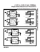
Figure 6 shows a graph of typical input current versus
input voltage.
Output Load Requirements
The MAX13013/MAX13014/MAX3023 I/O are designed to
drive CMOS inputs. Do not load the I/O lines with a resis-
tive load less than 25kΩ. Also, do not place an RC circuit
at the input of these devices to slow down the edges. If a
slower rise/fall time is required, refer to the
MAX3000E/MAX3001E logic-level-translators data sheet.
For I
2
C level translation, refer to the MAX3372E-
MAX3379E/MAX3390E–MAX3393E data sheet.
Enable Inputs
The MAX13013 single-, the MAX13014 dual- and the
MAX3023 (UCSP package) quad-level translators feature
an EN input. The MAX3023 (TSSOP package) quad-level
translator features both EN and EN inputs (see Table 2
for operating mode). Note that the MAX3023 (TSSOP
package) has internal pullup and pulldown circuitry on
EN and EN, respectively. If left unconnected, EN is pulled
up to V
L
and EN is pulled down to GND.
Applications Information
Power-Supply Decoupling
To reduce ripple and the chance of introducing data
errors, bypass V
L
and V
CC
to ground with a 0.1µF
ceramic capacitor. Place all capacitors as close to the
power-supply inputs as possible.
Unidirectional vs. Bidirectional Level
Translator
The MAX13013/MAX13014/MAX3023 bidirectional
translators can operate as a unidirectional device to
translate signals without inversion. These devices pro-
vide the smallest solution (UCSP package) for unidirec-
tional level translation without inversion.
UCSP Applications Information
For the latest application details on UCSP construction,
dimensions, tape carrier information, PC board tech-
niques, bump-pad layout, and recommended reflow tem-
perature profiles, as well as the latest information on
reliability testing results, go to Maxim’s web site at
www.maxim-ic.com/ucsp to find the Application Note:
UCSP—A Wafer-Level Chip-Scale Package.
Table 2. MAX3023 (TSSOP Package)
Operating Mode
EN
EN
O PER A T IN G M OD E
0 0 Both I/O V
L
_ and I/O V
CC
_ are in tri-state.
V
L
0 Normal operation.
0V
L
Both I/O V
L
_ and I/O V
CC
_ are in tri-state.
V
L
V
L
Both I/O V
L
_ and I/O V
CC
_ are in tri-state.
V
IN
V
TH_IN
/ R
IN
*
-(V
S
- V
TH_IN
) /
R
IN
*
I
IN
V
S
WHERE V
S
= V
CC
OR V
L
*R
IN
= 4kΩ WHEN DRIVING V
L
SIDE; R
IN
= 150Ω WHEN DRIVING V
CC
SIDE.
0
V
TH_IN
Figure 6. Typical I
IN
vs. V
IN