
Datasheet
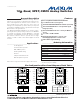

MAX312/MAX313/MAX314
10
ΩΩ
, Quad, SPST, CMOS Analog Switches
2 _______________________________________________________________________________________
ABSOLUTE MAXIMUM RATINGS
ELECTRICAL CHARACTERISTICS—Dual Supplies
(V+ = 15V, V- = -15V, VL = 5V, GND = 0V, V
INH
= 2.4V, V
INL
= 0.8V, T
A
= T
MIN
to T
MAX
, unless otherwise noted.)
Stresses beyond those listed under “Absolute Maximum Ratings” may cause permanent damage to the device. These are stress ratings only, and functional
operation of the device at these or any other conditions beyond those indicated in the operational sections of the specifications is not implied. Exposure to
absolute maximum rating conditions for extended periods may affect device reliability.
Voltages Referenced to GND
V+ ...........................................................................-0.3V to +44V
V- ............................................................................+0.3V to -44V
V+ to V-...................................................................-0.3V to +44V
VL .....................................................(GND - 0.3V) to (V+ + 0.3V)
All Other Pins (Note 1) ................................(V- - 2V) to (V+ + 2V)
or 30mA (whichever occurs first)
Continuous Current (COM_, NO_, NC_).........................±100mA
Peak Current (COM_, NO_, NC_) ...................................±300mA
Continuous Power Dissipation (T
A
= +70°C)
Plastic DIP (derate 10.53mW/°C above +70°C) ..........842mW
Narrow SO (derate 8.70mW/°C above +70°C) ............696mW
CERDIP (derate 10.00mW/°C above +70°C)...............800mW
TSSOP (derate 6.7mW/°C above +70°C) ....................457mW
Operating Temperature Ranges
MAX31_C_ ..........................................................0°C to +70°C
MAX31_E_ .......................................................-40°C to +85°C
MAX31_M_.....................................................-55°C to +125°C
Storage Temperature Range .............................-65°C to +150°C
Lead Temperature (soldering, 10s) .................................+300°C
Note 1: Signals on NC_, NO_, COM_, or IN_ exceeding V+ or V- will be clamped by internal diodes. Limit forward diode current to
maximum current rating.
(Note 3)
V
COM
= ±10V,
V
NO
_ or V
NC
_ = ±10V
I
COM
= 10mA,
V
NO
_ or V
NC
_ = ±10V
I
COM
= 10mA,
V
NO
_ or V
NC
_ = ±10V
CONDITIONS
6.5 10
VV- V+
V
COM
_,
V
NO
_,
V
NC
_
Analog Signal Range
nA
-40 40
I
NO
I
NC
Off Leakage Current
(NO_ or NC_)
(Note 6)
-2.5 2.5
-0.5 -0.02 0.5
9 Ω
15
R
ON
On-Resistance
0.3 1.5
Ω
3
ΔR
ON
On-Resistance Match Between
Channels (Note 4)
UNITS
MIN TYP MAX
(Note 2)
SYMBOLPARAMETER
C, E
M
T
A
=
+25°C
T
A
= T
MIN
to T
MAX
T
A
= +25°C
T
A
= T
MIN
to T
MAX
T
A
= +25°C
T
A
= T
MIN
to T
MAX
I
COM
= 10mA,
V
NO
_ or V
NC
_ = -5V,
0V, 5V
0.2 2
Ω
4
R
FLAT(ON)
On-Resistance Flatness
(Note 5)
T
A
= +25°C
T
A
= T
MIN
to T
MAX
C, E
M
V
COM
= ±10V,
V
NO
_ or V
NC
_ = ±10V
T
A
= +25°C
T
A
= T
MIN
to T
MAX
C, E
M
nA
-40 40
I
NC(OFF)
COM Off Leakage Current
(Note 6)
-2.5 2.5
-0.5 -0.02 0.5
V
COM
= ±10V,
V
NO
_ or V
NC
_ = ±10V
T
A
= +25°C
T
A
= T
MIN
to T
MAX
C, E
M
nA
-100 100
I
COM(ON)
COM On Leakage Current
(Note 6)
-5 5
-1 -0.04 1
ANALOG SWITCH