
Datasheet

__________Applications Information
Low-Distortion Audio
The MAX312/MAX313/MAX314, having very low R
ON
and very low R
ON
variation with signal amplitude, are
well suited for low-distortion audio applications. The
Typical Operating Characteristics
show Total Harmonic
Distortion (THD) vs. Frequency graphs for several sig-
nal amplitudes and impedances. Higher source and
load impedances improve THD, but reduce off isolation.
Off Isolation at High Frequencies
In 50Ω systems, the high-frequency on-response of
these parts extends from DC to above 100MHz with a
typical loss of -2dB. When the switch is turned off, how-
ever, it behaves like a capacitor, and off isolation
decreases with increasing frequency. (Above 300MHz,
the switch actually passes more signal turned off than
turned on.) This effect is more pronounced with higher
source and load impedances.
Above 5MHz, circuit board layout becomes critical, and
it becomes difficult to characterize the response of the
switch independent of the circuit. The graphs shown in
the
Typical Operating Characteristics
were taken using
a 50Ω source and load connected with BNC connec-
tors to a circuit board deemed “average”; that is,
designed with isolation in mind, but not using strip-line
or other special RF circuit techniques. For critical appli-
cations above 5MHz, use the MAX440, MAX441, and
MAX442, which are fully characterized up to 160MHz.
MAX312/MAX313/MAX314
10
ΩΩ
, Quad, SPST, CMOS Analog Switches
_______________________________________________________________________________________ 7
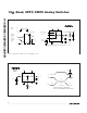
V+
COM_
V-
NO_
V
g
V+
V-
t
r
< 20ns
t
f
< 20ns
50%
0V
LOGIC
INPUT
V-
-15V
R
L
300Ω
NO1
OR NC1
GND
C
L
INCLUDES FIXTURE AND STRAY CAPACITANCE.
V
O
= V
COM (
RL
)
RL + RON
SWITCH
INPUT
IN1
+3V
t
OFF
0V
COM1
SWITCH
OUTPUT
0.9V
0
0.9V
0
t
ON
V
O
SWITCH
OUTPUT
LOGIC
INPUT
LOGIC INPUT WAVEFORMS INVERTED FOR SWITCHES
THAT HAVE THE OPPOSITE LOGIC SENSE.
VL
V+
C
L
35pF
+5V
+15V
V
O
V
COM1
0V
REPEAT TEST FOR EACH SWITCH. FOR LOAD
CONDITIONS, SEE Electrical Characteristics.
MAX312
MAX313
MAX314
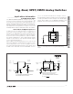
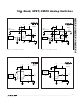
Figure 1. Overvoltage Protection Using External Blocking
Diodes
Figure 2. Switching-Time Test Circuit