
Datasheet


MAX3202E/MAX3203E/MAX3204E/MAX3206E
Low-Capacitance, 2/3/4/6-Channel, ±15kV ESD
Protection Arrays for High-Speed Data Interfaces
_______________________________________________________________________________________ 5
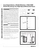
During an ESD event, the current pulse rises from zero
to peak value in nanoseconds (Figure 3). For example,
in a 15kV IEC-61000 Air-Gap Discharge ESD event,
the pulse current rises to approximately 45A in 1ns
(di/dt = 45 x 10
9
). An inductance of only 10nH adds an
additional 450V to the clamp voltage. An inductance of
10nH represents approximately 0.5in of board trace.
Regardless of the device’s specified diode clamp volt-
age, a poor layout with parasitic inductance significantly
increases the effective clamp voltage at the protected
signal line.
A low-ESR 0.1µF capacitor must be used between V
CC
and GND. This bypass capacitor absorbs the charge
transferred by an +8kV IEC-61000 Contact Discharge
ESD event.
Ideally, the supply rail (V
CC
) would absorb the charge
caused by a positive ESD strike without changing its
regulated value. In reality, all power supplies have an
effective output impedance on their positive rails. If a
power supply’s effective output impedance is 1Ω, then
by using V = I × R, the clamping voltage of V
C
increas-
es by the equation V
C
= I
ESD
x R
OUT
. An +8kV IEC
61000-4-2 ESD event generates a current spike of 24A,
so the clamping voltage increases by V
C
= 24A × 1Ω,
or V
C
= 24V. Again, a poor layout without proper
bypassing increases the clamping voltage. A ceramic
chip capacitor mounted as close to the MAX3202E/
MAX3203E/MAX3204E/MAX3206E V
CC
pin is the best
choice for this application. A bypass capacitor should
also be placed as close to the protected device as
possible.
±15kV ESD Protection
ESD protection can be tested in various ways; the
MAX3202E/MAX3203E/MAX3204E/MAX3206E are
characterized for protection to the following limits:
• ±15kV using the Human Body Model
• ±8kV using the Contact Discharge method speci-
fied in IEC 61000-4-2
• ±15kV using the IEC 61000-4-2 Air-Gap Discharge
method
ESD Test Conditions
ESD performance depends on a number of conditions.
Contact Maxim for a reliability report that documents
test setup, methodology, and results.
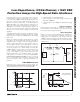
Human Body Model
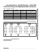
Figure 4 shows the Human Body Model, and Figure 5
shows the current waveform it generates when dis-
charged into a low impedance. This model consists of
a 100pF capacitor charged to the ESD voltage of inter-
est, which is then discharged into the device through a
1.5kΩ resistor.
CHARGE-CURRENT-
LIMIT RESISTOR
DISCHARGE
RESISTANCE
STORAGE
CAPACITOR
C
s
100pF
R
C
1MΩ
R
D
1.5kΩ
HIGH-
VOLTAGE
DC
SOURCE
DEVICE
UNDER
TEST
Figure 4. Human Body ESD Test Model
I
P
100%
90%
36.8%
t
RL
TIME
t
DL
CURRENT WAVEFORM
PEAK-TO-PEAK RINGING
(NOT DRAWN TO SCALE)
I
r
10%
0
0
AMPERES
Figure 5. Human Body Model Current Waveform
t
R
= 0.7ns to 1ns
30ns
60ns
t
100%
90%
10%
I
PEAK
I
Figure 3. IEC 61000-4-2 ESD Generator Current Waveform