
Datasheet


MAX3205E/MAX3207E/MAX3208E
Dual, Quad, and Hex High-Speed
Differential ESD-Protection ICs
_______________________________________________________________________________________
3
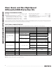
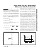
CLAMP VOLTAGE
vs. DC CURRENT
MAX3205E toc01
DC CURRENT (mA)
CLAMP VOLTAGE (V)
13011090705030
0.5
0.7
0.9
1.1
1.3
1.5
0.3
10 150
I/O_ TO V
CC
GND TO I/O_
LEAKAGE CURRENT
vs. TEMPERATURE
MAX3205E toc02
TEMPERATURE (°C)
LEAKAGE CURRENT (pA)
80400
10
100
1000
10,000
1
-40 120
INPUT CAPACITANCE
vs. INPUT VOLTAGE
MAX3205E toc03
INPUT VOLTAGE (V)
INPUT CAPACITANCE (pF)
4321
1
2
3
4
0
05
Typical Operating Characteristics
(V
CC
= +5V, T
A
= +25°C, unless otherwise noted.)
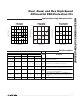
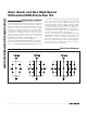
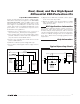
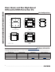
Pin Description
PIN
MAX3205E MAX3207E MAX3208E
TQFN-EP WLP SOT23 μMAX TQFN-EP
NAME FUNCTION
4, 5, 7,
12, 13, 15
A2, A3, B1,
B3, C1, C2
1, 4 1, 4, 6, 9 4, 7, 12, 15 I/O_ ESD-Protected Channel
1, 3, 6, 8,
9, 11, 14,
16
— 3, 6 2, 5, 7, 10
1, 3, 5, 6,
8, 9, 11,
13, 14, 16
N.C. No Connection. Not internally connected.
— B2 — — — N.C.
No Connection. The solder sphere is omitted from
this location (see the Package Information section).
2 A1 2 3 2 GND
Ground. Connect GND with a low-impedance
connection to the ground plane.
10 C3 5 8 10 V
CC
Power-Supply Input. Bypass V
CC
to GND with a
0.1μF ceramic capacitor as close to the device as
possible.
— — — — — EP Exposed Pad (TQFN Only). Connect EP to GND.