
Datasheet


Applications Information
Design Considerations
Maximum protection against ESD damage results from
proper board layout (see the
Layout Recommendations
section). A good layout reduces the parasitic series
inductance on the ground line, supply line, and protect-
ed signal lines. The MAX3205E/MAX3207E/MAX3208E
ESD diodes clamp the voltage on the protected lines
during an ESD event and shunt the current to GND or
V
CC
. In an ideal circuit, the clamping voltage (V
C
) is
defined as the forward voltage drop (V
F
) of the protec-
tion diode, plus any supply voltage present on the cath-
ode.
For positive ESD pulses:
V
C
= V
CC
+ V
F
For negative ESD pulses:
V
C
=-V
F
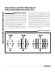
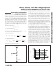
The effect of the parasitic series inductance on the
lines must also be considered (Figure 1).
For positive ESD pulses:
For negative ESD pulses:
where I
ESD
is the ESD current pulse.
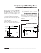
During an ESD event, the current pulse rises from zero
to peak value in nanoseconds (Figure 2). For example,
in a 15kV IEC 61000 Air-Gap Discharge ESD event, the
pulse current rises to approximately 45A in 1ns (di/dt =
45 x 10
9
). An inductance of only 10nH adds an addi-
tional 450V to the clamp voltage and represents
approximately 0.5in of board trace. Regardless of the
device’s specified diode clamp voltage, a poor layout
with parasitic inductance significantly increases the
effective clamp voltage at the protected signal line.
Minimize the effects of parasitic inductance by placing
the MAX3205E/MAX3207E/MAX3208E as close to the
connector (or ESD contact point) as possible.
A low-ESR 0.1µF capacitor is recommended between
V
CC
and GND in order to get the maximum ESD protec-
tion possible. This bypass capacitor absorbs the
charge transferred by a positive ESD event. Ideally, the
supply rail (V
CC
) would absorb the charge caused by a
positive ESD strike without changing its regulated
value. All power supplies have an effective output
impedance on their positive rails. If a power supply’s
effective output impedance is 1Ω, then by using V = I x
R, the clamping voltage of V
C
increases by the equa-
tion V
C
= I
ESD
x R
OUT
. A +8kV IEC 61000-4-2 ESD
event generates a current spike of 24A. The clamping
voltage increases by V
C
= 24A x 1Ω, or V
C
= 24V.
Again, a poor layout without proper bypassing increas-
es the clamping voltage. A ceramic chip capacitor
mounted as close as possible to the MAX3205E/
MAX3207E/MAX3208E V
CC
pin is the best choice for
this application. A bypass capacitor should also be
placed as close to the protected device as possible.
VV Lx
dI
dt
Lx
dI
dt
CFD
ESD ESD
()
()
=− +
⎛
⎝
⎜
⎞
⎠
⎟
+
⎛
⎝
⎜
⎞
⎠
⎟
⎛
⎝
⎜
⎞
⎠
⎟
()
2
13
VV V Lx
dI
dt
Lx
dI
dt
CCCFD
ESD ESD
()
()
=+ +
⎛
⎝
⎜
⎞
⎠
⎟
+
⎛
⎝
⎜
⎞
⎠
⎟
()
1
12
MAX3205E/MAX3207E/MAX3208E
Dual, Quad, and Hex High-Speed
Differential ESD-Protection ICs
_______________________________________________________________________________________ 5
L1
PROTECTED
LINE
L3
D2
GROUND RAIL
POSITIVE SUPPLY RAIL
I/O_
D1
L2
Figure 1. Parasitic Series Inductance
t
R
= 0.7ns to 1ns
30ns
60ns
t
100%
90%
10%
I
PEAK
I
Figure 2. IEC 61000-4-2 ESD Generator Current Waveform