
Datasheet


Layout Recommendations
Proper circuit-board layout is critical to suppress ESD-
induced line transients (See Figure 6). The MAX3205E/
MAX3207E/MAX3208E clamp to 100V; however, with
improper layout, the voltage spike at the device can be
much higher. A lead inductance of 10nH with a 45A
current spike results in an additional 450V spike on the
protected line. It is essential that the layout of the PC
board follows these guidelines:
1) Minimize trace length between the connector or
input terminal, I/O_, and the protected signal line.
2) Use separate planes for power and ground to reduce
parasitic inductance and to reduce the impedance to
the power rails for shunted ESD current.
3) Ensure short low-inductance ESD transient return
paths to GND and V
CC
.
4) Minimize conductive power and ground loops.
5) Do not place critical signals near the edge of the PC
board.
6) Bypass V
CC
to GND with a low-ESR ceramic capaci-
tor as close to V
CC
as possible.
7) Bypass the supply of the protected device to GND
with a low-ESR ceramic capacitor as close to the
supply pin as possible.
WLP Applications Information
For the latest application details on WLP construction,
dimensions, tape carrier information, printed circuit
board techniques, bump-pad layout, and recommend-
ed reflow temperature profile, as well as the latest infor-
mation on reliability testing results, refer to Application
Note 1891:
Wafer-Level Packaging (WLP) and Its
Applications
.
Chip Information
PROCESS: BiCMOS
MAX3205E/MAX3207E/MAX3208E
Dual, Quad, and Hex High-Speed
Differential ESD-Protection ICs
_______________________________________________________________________________________ 7
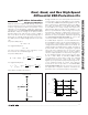
V
CC
PROTECTED LINE
NEGATIVE ESD-
CURRENT
PULSE
PATH TO
GROUND
PROTECTED
CIRCUIT
GND
D1
I/O_
V
C
D2
L1
L3
L2
Figure 6. Layout Considerations
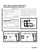
MAX3205E
MAX3207E
MAX3208E
0.1μF
0.1μF
I/0_
I/0
I/0 LINE
V
CC
V
CC
PROTECTED
CIRCUIT
Typical Operating Circuit