
Datasheet


MAX3372E–MAX3379E/MAX3390E–MAX3393E
±15kV ESD-Protected, 1µA, 16Mbps, Dual/Quad
Low-Voltage Level Translators in UCSP
11
Maxim Integrated
Level Translation
For proper operation ensure that +1.65V ≤ V
CC
≤
+5.5V, +1.2V ≤ V
L
≤ +5.5V, and V
L
≤ (V
CC
+ 0.3V).
During power-up sequencing, V
L
≥ (V
CC
+ 0.3V) will
not damage the device. During power-supply sequenc-
ing, when V
CC
is floating and V
L
is powering up, a cur-
rent may be sourced, yet the device will not latch up.
The speed-up circuitry limits the maximum data rate for
devices in the MAX3372E–MAX3379E, MAX3390E–
MAX3393E family to 16Mbps. The maximum data rate
also depends heavily on the load capacitance (see the
Typical Operating Characteristics
), output impedance
of the driver, and the operational voltage range (see the
Timing Characteristics
table)
.
Speed-Up Circuitry
The MAX3373E–MAX3376E/MAX3378E/MAX3379E and
MAX3390E–MAX3393E feature a one-shot generator that
decreases the rise time of the output. When triggered,
MOSFETs PU1 and PU2 turn on for a short time to pull up
I/O V
L_
and I/O V
CC_
to their respective supplies (see
Figure 2b). This greatly reduces the rise time and propa-
gation delay for the low-to-high transition. The scope
photo of Rail-to-Rail Driving for 8Mbps Operation in the
Typical Operating Characteristics
shows the speed-up
circuitry in operation.
Rise-Time Accelerators
The MAX3373E–MAX3376E/MAX3378E/MAX3379E and
the MAX3390E–MAX3393E have internal rise-time
accelerators allowing operation up to 16Mbps. The
rise-time accelerators are present on both sides of the
device and act to speed up the rise time of the input
and output of the device, regardless of the direction of
the data. The triggering mechanism for these accelera-
tors is both level and edge sensitive. To prevent false
triggering of the rise-time accelerators, signal fall times
of less than 20ns/V are recommended for both the
inputs and outputs of the device. Under less noisy con-
ditions, longer signal fall times may be acceptable.
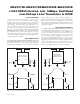
MAX3372E–MAX3379E
AND MAX3390E–MAX3393E
I/O V
L_
I/O V
CC_
V
CC
V
CC
V
L
V
L
GND
I/O V
CC_
t
PD-VCC-LH
t
PD-VCC-HL
I/O V
L_
t
RVCC
t
FVCC
DATA
R
LOAD
C
LOAD
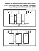
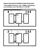
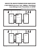
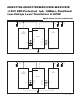
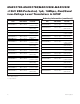
Figure 1c. Open-Drain Driving I/O V
CC
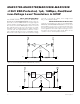
MAX3373E–MAX3376E,
MAX3378E/MAX3379E
AND MAX3390E–MAX3393E
I/O V
L_
I/O V
CC_
DATA
I/O V
CC_
V
CC
V
CC
V
L
V
L
GND
R
LOAD
C
LOAD
t
PD-VL-LH
t
PD-VL-HL
I/O V
L_
t
RVL
t
FVL
Figure 1d. Open-Drain Driving I/O V
L