
Datasheet
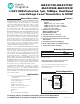


MAX3372E–MAX3379E/MAX3390E–MAX3393E
±15kV ESD-Protected, 1µA, 16Mbps, Dual/Quad
Low-Voltage Level Translators in UCSP
4
Maxim Integrated
TIMING CHARACTERISTICS
(V
CC
= +1.65V to +5.5V, V
L
= +1.2V to (V
CC
+ 0.3V), GND = 0, R
LOAD
= 1MΩ, I/O test signal of Figure 1, T
A
= T
MIN
to T
MAX
, unless
otherwise noted. Typical values are at V
CC
= +3.3V, V
L
= +1.8V, T
A
= +25°C, unless otherwise noted.) (Notes 1, 2)
PARAMETER SYM B O L CONDITIONS MIN TYP MAX UNITS
MAX3372E/MAX3377E (C
LOAD
= 50pF)
I/O V
CC
_ Rise Time (Note 4) t
RVCC
1100 ns
I/O V
CC
_ Fall Time (Note 5) t
FVCC
1000 ns
I/O V
L
_ Rise Time (Note 4) t
RVL
600 ns
I/O V
L
_ Fall Time (Note 5) t
FVL
1100 ns
I/O
VL-VCC
Driving I/O V
L
_ 1.6
Propagation Delay
I/O
VCC-VL
Driving I/O V
CC
_ 1.6
µs
Channel-to-Channel Skew t
SKEW
Each translator equally loaded 500 ns
Maximum Data Rate C
L
= 25pF 230 kbps
M A X3 3 7 3 E– M A X3 3 7 6 E/M A X3 3 7 8 E/ M A X3 3 7 9 E a n d M A X3 3 9 0 E– M A X3 3 9 3 E ( C
LOA D
= 15 p F , Dr iv e r O u t p u t Im p e d a n c e ≤ 5 0 Ω)
+1.2V ≤ V
L
≤ V
CC
≤ +5.5V
725
I/O V
CC
_ Rise Time (Note 4) t
RVCC
Open-drain driving 170 400
ns
637
I/O V
CC
_ Fall Time (Note 5) t
FVCC
Open-drain driving 20 50
ns
830
I/O V
L
_ Rise Time (Note 4) t
RVL
Open-drain driving 180 400
ns
330
I/O V
L
_ Fall Time (Note 5) t
LFV
Open-drain driving 30 60
ns
530
I/O
VL-VCC
Driving I/O V
L
_
Open-drain driving 210 1000
430
Propagation Delay
I/O
VCC-VL
Driving I/O V
CC
_
Open-drain driving 190 1000
ns
20
Channel-to-Channel Skew t
SKEW
Each translator
equally loaded
Open-drain driving 50
ns
8 Mbps
Maximum Data Rate
Open-drain driving 500 kbps