
Datasheet


MAX3394E/MAX3395E/MAX3396E
Power-Supply Sequencing
The MAX3394E/MAX3395E/MAX3396E require two sup-
ply voltages. For proper operation, ensure that +1.65V ≤
V
CC
≤ +5.5V, and +1.2V ≤ V
L
≤ V
CC
. There are no restric-
tions on power-supply sequencing. During power-up or
power-down, the MAX3394E/MAX3395E/MAX3396E can
withstand either the V
L
or the V
CC
supply floating while
the other supply is applied. The device will not latch up in
this state.
Tri-State Output Mode
Connect EN to V
L
or V
CC
for normal operation. Drive
EN low to force the MAX3394E/MAX3395E/MAX3396E
to a tri-state output mode. In tri-state output mode, all
I/O lines are driven to a high-impedance state, and the
pass-FET is disabled to prevent current flow between
I/O lines. Tri-state output mode disables the internal
pullup resistors on I/O V
L
_ and I/O V
CC
_, and reduces
supply current to 3µA typ (V
CC
) and 0.7µA typ (V
L
).
±15kV ESD-Protected, High-Drive Current, Dual-/Quad-/
Octal-Level Translators with Speed-Up Circuitry
10 ______________________________________________________________________________________
MAX3394E
MAX3395E
MAX3396E
I/O V
L_
I/O V
CC_
V
L
V
L
V
CC
V
CC
V
L
V
CC
EN
50Ω
R
LOAD
C
IOVCC
MAX3394E
MAX3395E
MAX3396E
I/O V
CC_
V
L
V
L
V
CC
V
CC
V
L
V
CC
EN
50Ω
R
LOAD
I/O V
L_
EN
EN
TIME
TIME
t
EN
t
EN
I/O V
CC_
V
I/O V
L_
V
C
IOVL
0.5V
0.2V (V
L
< 2V)
0.5V (V
L
≥ 2V)
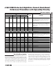
Figure 5. Enable Test Circuit and Timing