
Datasheet


MAX3394E/MAX3395E/MAX3396E
±15kV ESD-Protected, High-Drive Current, Dual-/Quad-/
Octal-Level Translators with Speed-Up Circuitry
2 _______________________________________________________________________________________
ABSOLUTE MAXIMUM RATINGS
Stresses beyond those listed under “Absolute Maximum Ratings” may cause permanent damage to the device. These are stress ratings only, and functional
operation of the device at these or any other conditions beyond those indicated in the operational sections of the specifications is not implied. Exposure to
absolute maximum rating conditions for extended periods may affect device reliability.
(All voltages referenced to GND.)
V
CC
......................................................................... -0.3V to +6V
V
L
............................................................................ -0.3V to +6V
I/O V
CC_
...................................................... -0.3V to V
CC
+ 0.3V
I/O V
L_
........................................................... -0.3V to V
L
+ 0.3V
EN ........................................................................... -0.3V to +6V
Short-Circuit Duration I/O V
L_
, I/O V
CC_
to GND ..... Continuous
Maximum Continuous Current ........................................ ±50mA
Continuous Power Dissipation (T
A
= +70°C)
8-Pin TDFN (derate 18.2mW/°C above +70°C) ........ 1455mW
9-Bump UCSP (derate 4.7mW/°C above +70°C) ........ 379mW
12-Pin TQFN (derate 16.9mW/°C above +70°C) ........1349mW
12-Bump UCSP (derate 6.5mW/°C above +70°C) ..... 519mW
20-Pin TQFN (derate 20.8mW/°C above +70°C) ........1667mW
20-Bump UCSP (derate 10.0mW/°C above +70°C) .....800mW
Operating Temperature Range ......................... -40°C to +85°C
Storage Temperature Range ........................... -65°C to +150°C
Junction Temperature .....................................................+150°C
Bump Temperature (soldering) ...................................... +235°C
Lead Temperature (soldering, 10s) ............................... +300°C
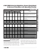
ELECTRICAL CHARACTERISTICS
(V
CC
= +1.65V to +5.5V, V
L
= +1.2V to V
CC
; C
IOVL
≤ 15pF, C
IOVCC
≤ 15pF; T
A
= -40°C to +85°C, unless otherwise noted. Typical val-
ues are at T
A
= +25°C.) (Note 1)
PARAMETER SYMBOL CONDITIONS MIN TYP MAX UNITS
POWER SUPPLY
V
L
Supply Range V
L
1.2 V
CC
V
V
CC
Supply Range V
CC
1.65 5.50 V
MAX3394E 150
MAX3395E 300Supply Current from V
CC
I
CC
I/O lines internally
pulled up
MAX3396E 600
µA
MAX3394E 30
MAX3395E 30
Supply Current from V
L
I
L
I/O lines internally
pulled up
MAX3396E 30
µA
V
CC
Tri-State Supply Current I
CC-3
EN = GND, T
A
= +25°C 3 6 µA
V
L
Tri-State Supply Current I
L-3
EN = GND, T
A
= +25°C 0.7 2 µA
LOGIC I/O
I/O V
L
_ Input-Voltage High
Threshold
V
IHL
0.7 x
V
L
V
I/O V
L
_ Input-Voltage Low
Threshold
V
ILL
0.3 x
V
L
V
I/O V
L
_ Internal Pullup DC
Resistance
R
L
EN = V
CC
or V
L
51020kΩ
I/O V
L
_ Source Current During
Low-to-High Transition
I
IHL
V
L
= +1.2V 15 mA
I/O V
L
_ Sink Current During High-
to-Low Transition
I
ILL
V
CC
= +1.65V 10 mA