
Datasheet


MAX3394E/MAX3395E/MAX3396E
±15kV ESD-Protected, High-Drive Current, Dual-/Quad-/
Octal-Level Translators with Speed-Up Circuitry
4 _______________________________________________________________________________________
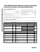
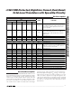
TIMING CHARACTERISTICS
(V
CC
= +1.65V to +5.5V, V
L
= +1.2V to V
CC
; C
IOVL
≤ 15pF, C
IOVCC
≤ 15pF; T
A
= -40°C to +85°C, unless otherwise noted. Typical val-
ues are at T
A
= +25°C.) (Note 1)
PARAMETER SYMBOL CONDITIONS MIN TYP MAX UNITS
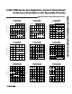
Push-pull driver, Figure 1 50
I/O V
CC
_ Rise Time t
RVCC
Open-drain driver, internal pullup, Figure 2 500
ns
Push-pull driver, Figure 1 50
I/O V
CC
_ Fall Time t
FVCC
Open-drain driver, internal pullup, Figure 2 50
ns
Push-pull driver, Figure 3 50
I/O V
L
_ Rise Time t
RVL
Open-drain driver, internal pullup, Figure 4 500
ns
Push-pull driver, Figure 3 50
I/O V
L
_ Fall Time t
FVL
Open-drain driver, internal pullup, Figure 4 50
ns
Push-pull driver, Figure 1 50
t
I/OVL-VCC
Open-drain driver, internal pullup, Figure 2 600
Push-pull driver, Figure 3 50
Propagation Delay
t
I/OVCC-VL
Open-drain driver, internal pullup, Figure 4 600
ns
Propagation Delay After EN t
EN
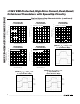
Push-pull or open-drain driver, Figure 5 5 µs
Push-pull driver 5
Channel-to-Channel Skew t
SKEW
Open-drain driver, internal pullup 100
ns
Push-pull driver, Figures 1, 3 6
Maximum Data Rate
Open-drain driver, internal pullup,
Figures 2, 4
1
Mbps
Note 1: All units are 100% production tested at T
A
= +25°C. Limits over the operating temperature range are guaranteed by design
and not production tested.
Note 2: During a low-to-high transition, the threshold at which the I/O changes state is the lower of V
ILL
and V
ILC
since the two sides
are internally connected by an internal switch while the device is in the logic-low state.