
Datasheet


General Description
The MAX3394E/MAX3395E/MAX3396E bidirectional
level translators provide level shifting required for data
transfer in a multivoltage system. Internal slew-rate
enhancement circuitry features 10mA current-sink and
15mA current-source drivers to isolate capacitive loads
from lower current drivers. In open-drain systems, slew-
rate enhancement enables fast data rates with larger
pullup resistors and increased bus load capacitance.
Externally applied voltages, V
CC
and V
L
, set the logic-
high levels for the device. A logic-low signal on one I/O
side of the device appears as a logic-low signal on the
opposite I/O side, and vice-versa. Each I/O line is
pulled up to V
CC
or V
L
by an internal pullup resistor,
allowing the devices to be driven by either push-pull or
open-drain drivers.
The MAX3394E/MAX3395E/MAX3396E feature a tri-
state output mode, thermal-shutdown protection, and
±15kV Human Body Model (HBM) ESD protection on
the V
CC
side for greater protection in applications that
route signals externally.
The MAX3394E/MAX3395E/MAX3396E accept V
CC
volt-
ages from +1.65V to +5.5V, and V
L
voltages from +1.2V
to V
CC
, making them ideal for data transfer between low
voltage ASIC/PLDs and higher voltage systems. The
MAX3394E/MAX3395E/MAX3396E operate at a guaran-
teed data rate of 6Mbps with push-pull drivers and
1Mbps with open-drain drivers.
The MAX3394E is a dual-level translator available in
9-bump UCSP™ and 8-pin 3mm x 3mm TDFN packages.
The MAX3395E is a quad-level translator available in 12-
bump UCSP, and 12-pin 4mm x 4mm TQFN packages.
The MAX3396E is an octal-level translator available in 20-
bump UCSP and 20-pin 5mm x 5mm TQFN packages.
The MAX3394E/MAX3395E/MAX3396E operate over the
extended -40°C to +85°C temperature range.
Applications
Multivoltage Bidirectional Level Translation
SPI™, MICROWIRE™, and I
2
C Level Translation
Open-Drain Rise-Time Speed-Up
High-Speed Bus Fan-Out Expansion
Cell Phones
Telecom, Networking, Servers, RAID/SAN
Features
♦ ±15kV ESD Protection on I/O V
CC_
Lines
♦ Bidirectional Level Translation Without Direction
Pin
♦ I/O V
L_
and I/O V
CC_
10mA Sink-/15mA Source-
Current Capability
♦ Slew-Rate Enhancement Circuitry Supports
Larger Capacitive Loads or Larger External Pullup
Resistors
♦ 6Mbps Push-Pull/1Mbps Open-Drain Guaranteed
Data Rate
♦ Wide Supply-Voltage Range: Operation Down to
+1.2V on V
L
and +1.65V on V
CC
♦ Low Supply Current in Tri-State Output Mode
(3µA typ)
♦ Low Quiescent Current
♦ Thermal-Shutdown Protection
♦ UCSP, TDFN, and TQFN Packages
MAX3394E/MAX3395E/MAX3396E
±15kV ESD-Protected, High-Drive Current, Dual-/Quad-/
Octal-Level Translators with Speed-Up Circuitry
________________________________________________________________
Maxim Integrated Products
1
19-3884; Rev 2; 2/07
For pricing, delivery, and ordering information, please contact Maxim/Dallas Direct! at
1-888-629-4642, or visit Maxim’s website at www.maxim-ic.com.
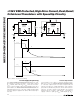
12
34
8
7
6
5
V
L
I/O V
L
1
I/O V
L
2
GND
*CONNECT EXPOSED PAD TO GROUND
*EP
I/O V
CC
2
I/O V
CC
1
EN
V
CC
MAX3394E
TDFN
TOP VIEW
(LEADS ON BOTTOM)
+
Pin Configurations
Ordering Information
PART PIN-PACKAGE PKG CODE
MAX3394EETA+T 8 TDFN-EP** T833-1
MAX3394EEBL+T 9 UCSP B9-5
MAX3395EETC+ 12 TQFN-EP** T1244-4
MAX3395EEBC+T 12 UCSP B12-1
MAX3396EEBP+T* 20 UCSP B20-1
MAX3396EETP+* 20 TQFN-EP** T2055-4
MICROWIRE is a trademark of National Semiconductor Corp.
SPI is a trademark of Motorola, Inc.
UCSP is a trademark of Maxim Integrated Products, Inc.
Note: All devices specified over the -40°C to +85°C operating
range.
+
Denotes lead(Pb)-free/RoHS-compliant package.
*
Future product—contact factory for availability.
**EP = Exposed paddle.
Pin Configurations continued at end of data sheet.
Selector Guide appears at end of data sheet.