
Datasheet
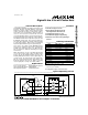


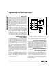

___________________Chip Topography
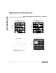
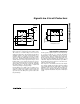
_________________Pin Configurations
V+
IN3
V-
0.112"
(2.84mm)
0.085"
(2.16mm)
OUT1
OUT2
OUT3
IN2
IN1
TRANSISTOR COUNT: 21
SUBSTRATE CONNECTED TO V+
IN4
IN3
IN2
IN1
IN7
IN6
IN5
18
17
16
15
14
13
12
11
1
2
3
4
5
6
7
8
V+
OUT1
OUT2
OUT3
DIP/SO
OUT4
OUT5
OUT6
OUT7
IN8
10
9
OUT8
V-
MAX367
V-
IN3
IN2
IN1
8
7
6
5
1
2
3
4
V+
OUT1
OUT2
OUT3
TOP VIEW
DIP/SO
MAX366
MAX366/MAX367
Signal-Line Circuit Protectors
10 ______________________________________________________________________________________
__High-Voltage Surge Suppression
These devices are not high-voltage arresters, nor are they
substitutes for surge suppressers. In systems that use
these forms of protection, however, the MAX366/MAX367
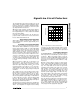
can fill a vital gap. Figure 7 shows a typical circuit.
Although the surge suppressers are extremely fast shunt
elements, they have very soft current knees. Their clamp
voltage must be chosen well above the normal signal
levels, because they have excessive leakage currents as
the knee is approached. This current can interfere with
normal operation when signal levels are low or imped-
ances are high. If the clamp voltage is too high, however,
the input can be damaged.
Using a MAX366/MAX367 after the surge suppresser
allows the surge-suppresser voltage to be set above
the supply voltage (but within the overvoltage limits),
dramatically reducing the effects of leakage (Figure 7).
During a surge, the surge suppresser clamps the input
voltage to
roughly
±10V. This protects the
MAX366/MAX367, but the MAX366/MAX367 still dis-
connect the signal from the op amp well within the ±5V
supply.
MAX366
OUT11 IN1 7
+5V
-5V
SURGE SUPPRESSERS
(+10V)
OUT22 IN2 6
OUT33 IN3 5
V+
4
V-
8
OP AMP
Figure 7. Surge-Suppression Circuit