
Datasheet


MAX366/MAX367
Signal-Line Circuit Protectors
_______________________________________________________________________________________ 5
___________Background Information
When a voltage outside the supply range is applied to
most integrated circuits, there is a strong possibility they
will be damaged or “latch up” (that is, fail to operate prop-
erly even after the offending voltage is removed). If an
IC’s input or output pin is supplied with a voltage when the
IC’s power is off, and power is subsequently applied, the
device may act as an SCR and destroy itself and/or other
circuitry. Such “faults” are commonly encountered in
modular control systems where power and signals to inter-
connected modules may be interrupted and re-estab-
lished at random. They can happen during production
testing, maintenance, start-up, or a power “brownout.”
The MAX366/MAX367 are designed to protect delicate
input and output circuitry from overvoltage faults up to
±40V (with or without power applied), in devices such as
op amps, analog-to-digital/digital-to-analog converters,
and voltage references. These circuit protectors automati-
cally limit signal voltages and currents to safe levels with-
out degrading normal signal performance, even in very
high-impedance circuits. They are powered by the power
supply of the protected circuit and inserted into the signal
lines. There are no control lines, programming pins, or
adjustments.
Unlike shunt diode networks, these devices are low-
impedance FETs that become high impedance during a
fault condition, so fault current and power dissipation are
extremely low. Equally important, leakage current during
normal and fault conditions is extremely low. In addition,
unlike most discrete networks, these parts protect circuits
both when power is off and during power transitions.
_______________Detailed Description
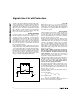
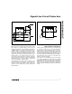
Internal Construction
Figure 1 shows the simplified internal construction of
each protector inside the MAX366/MAX367. Each circuit
consists of two N-channel FETs and one P-channel FET.
All the FETs are enhancement types; that is, the N chan-
nels must have approximately 1.3V of positive gate volt-
age in order to conduct, and the P channel must have
approximately 2V of negative gate voltage in order to
conduct.
During normal operation, V+ is connected to a positive
potential and V- is connected to a negative potential.
Since their gates are tied to V+, transistors Q1 and Q3
conduct as long as their sources are at least 1.3V below
V+ (the N-channel gate threshold.) Transistor Q2’s gate
is tied to V-, so it conducts as long as its source is 2V or
more above V- (the P-channel gate threshold.)
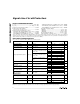
______________________________________________________________Pin Description
PIN
MAX366 MAX367
FUNCTION
1, 2, 3 1, 2, 3 Signal Inputs 1, 2, 3
– 4–8 Signal Inputs 4–8
4 9 Negative Supply Voltage Input
NAME*
IN1, IN2, IN3
8 18 Positive Supply Voltage Input
– 10–14 Signal Outputs 4–8
IN4–IN8
V-
V+
OUT8–OUT4
5, 6, 7 15, 16, 17 Signal Outputs 1, 2, 3
OUT3, OUT2,
OUT1
* Inputs and outputs are names for convenience only; inputs and outputs are identical and interchangeable.
P
Q2
N
Q3
N
Q1
OUT
V+
V-
IN
Figure 1. Simplified Internal Structure