
Datasheet


MAX366/MAX367
Signal-Line Circuit Protectors
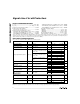
_______________________________________________________________________________________ 9
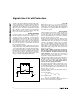
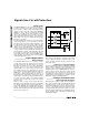
Figure 6 shows a circuit that can give reliable results.
This circuit uses a 100mV voltage source and a low-
voltage-drop ammeter as the measuring circuit, and an
adjustable supply to sweep the analog voltage across
its whole range. The ammeter must have a voltage
drop of less than one millivolt (at any current) for accu-
rate results. (A Keithley Model 617 Electrometer has a
suitable ammeter circuit, appropriate ranges, and a
built-in voltage source designed for this type of mea-
surement.) Measurements are made by setting the
analog voltage, measuring the current, and calculating
the path resistance. The procedure is repeated at
each analog voltage and supply voltage.
It is important to use a voltage source of 100mV or less.
As shown in Figure 4, this voltage is added to the V
IN
voltage to form the V
OUT
voltage. Using a higher volt-
age could cause the OUT pin to go into a fault condi-
tion prematurely.
High-Frequency Performance
In 50Ω systems, signal response is reasonably flat up
to several megahertz (see
Typical Operating
Characteristics
). Above 5MHz, the response has sev-
eral minor peaks, which are highly layout dependent.
Because the path resistance is dependent on the sup-
ply voltage and signal amplitude, the impedance is not
controlled. Adjacent channel attenuation up to 5MHz is
about 3dB above that of a bare IC socket, and is due
entirely to capacitive coupling.
Pulse response is reasonable, but because the imped-
ance changes rapidly, fast rise times may induce ringing
as the signal approaches the fault voltage. At very high
amplitudes (such as noise spikes), the capacitive cou-
pling across the signal pins will transfer considerable
energy, despite the fact that the DC path is a virtual open
circuit.
MAX366
OUT_V
IN
4
IN_ V
OUT
V+
V-
V+
V-
PATH RESISTANCE = 100mV/A
100mV
ADJUSTABLE ANALOG VOLTAGE
8
A
Figure 6. Path-Resistance Measuring Circuit
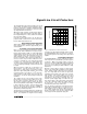
MAX366
OUT11 IN1 7
+5V
-5V
OUT22 IN2 6
OUT33 IN3 5
V+
4
V-
8
P
100k
SWITCHED +5V
OP AMP
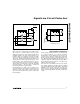
Figure 5. Power-Supply Sequencing