
Datasheet


MAX3869
should equal 25Ω. Typical values for R
D
are 18Ω to
23Ω. For best performance, a bypass capacitor (0.01µF
typical) should be placed as close as possible to the
anode of the laser diode. Depending on the exact char-
acteristics of the laser diode and PC board layout, a
resistor (R
P
) of 20Ω to 70Ω in parallel with pull-up induc-
tor L
P1
can be useful in damping overshoot and ringing
in the optical output.
In some applications (depending on laser-diode para-
sitic inductance characteristics), an RC shunt network
between the laser cathode and ground will help mini-
mize optical output aberrations. Starting values for most
coaxial lasers are R = 75Ω in series with C = 3.3pF.
These values should be experimentally adjusted until
the optical output waveform is optimized.
Pattern-Dependent Jitter
When transmitting NRZ data with long strings of con-
secutive identical digits (CIDs), LF droop can occur
and contribute to pattern-dependent jitter (PDJ). To
minimize this PDJ, three external components must be
properly chosen: capacitor C
APC
, which dominates the
APC loop time constant; pull-up inductor L
P
; and AC-
coupling capacitor C
D
.
To filter out noise effects and guarantee loop stability,
the recommended value for C
APC
is 0.1µF. This results
in an APC loop bandwidth of 10kHz or a time constant
of 16µs. As a result, the PDJ associated with an APC
loop time constant can be ignored.
The time constant associated with the output pull-up
inductor (L
P
≈
L
P2
), and the AC-coupling capacitor (C
D
)
will also impact the PDJ. For such a second-order net-
work, the PDJ due to the low frequency cutoff will be
dominated by L
P
. For a data rate of 2.5Gbps, the rec-
ommended value for C
D
is 0.056µF. During the maxi-
mum CID period
,
it is recommended to limit the peak
voltage droop to less than 12% of the average (6% of
the amplitude). The time constant can be estimated by:
12% = 1 - e
-t
/
τ
L
P
τ
LP
= 7.8t
If τ
LP
= L
P
/ 25Ω, and t = 100UI = 40ns, then L
P
= 7.8µH.
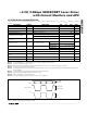
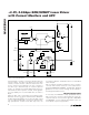
To reduce the physical size of this element (L
P
), use of
SMD ferrite beads is recommended (Figure 2).
Input Termination Requirement
The MAX3869 data and clock inputs are PECL compat-
ible. However, it is not necessary to drive the MAX3869
with a standard PECL signal. As long as the specified
common-mode voltage and the differential voltage
swings are met, the MAX3869 will operate properly.
Calculating Power Consumption
The junction temperature of the MAX3869 dice must be
kept below +150°C at all times. The total power dissipa-
tion of the MAX3869 can be estimated by the following:
P = V
CC
✕ I
CC
+ (V
CC
- V
f
) ✕ I
BIAS
+ I
MOD
(V
CC
- 25Ω ✕ I
MOD
/ 2)
where I
BIAS
is the maximum bias current set by R
BIAS-
MAX
, I
MOD
is the modulation current, and V
f
is the typi-
cal laser forward voltage.
Junction Temperature = P(W) ✕ 45 (°C/W)
___________Applications Information
An example of how to set up the MAX3869 follows.
Select Laser
A communication-grade laser should be selected for
2.488Gbps applications. Assume the laser output aver-
age power is P
AVG
= 0dBm, minimum extinction ratio is
r
e
= 6.6 (8.2dB), the operating temperature is -40°C to
+85°C, and the laser diode has the following character-
istics:
Wavelength: λ = 1.3µm
Threshold Current: Ι
TH
= 22mA at +25°C
Threshold Temperature
Coefficient: β
TH
= 1.3%/°C
Laser to Monitor Transfer: ρ
MON
= 0.2A/W
Laser Slope Efficiency: η = 0.05mW/mA
at +25°C
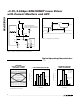
Determine R
APCSET
The desired monitor diode current is estimated by
I
MD
= P
AVG
·
ρ
MON
= 200µA. The I
MD
vs. R
APCSET
graph in the Typical Operating Characteristics shows
that R
APCSET
should be 6.0kΩ.
Determine R
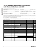
MODSET
To achieve a minimum extinction ratio (r
e
) of 6.6 over
temperature and lifetime, calculate the required extinc-
tion ratio at +25°C. Assuming r
e
= 20, the peak-to-peak
optical power P
p-p
= 1.81mW, according to Table 1. The
required modulation current is 1.81(mW) / 0.05(mW/mA)
= 36.2mA. The I
MOD
vs. R
MODSET
graph in the Typical
Operating Characteristics shows that R
MODSET
should
be 4.8kΩ.
+3.3V, 2.5Gbps SDH/SONET Laser Driver
with Current Monitors and APC
10 ______________________________________________________________________________________