
Datasheet


MAX3869
+3.3V, 2.5Gbps SDH/SONET Laser Driver
with Current Monitors and APC
6 _______________________________________________________________________________________
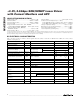
Pin Description
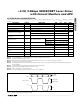
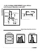
Typical Operating Characteristics (continued)
(V
CC
= +3.3V, load as shown in Figure 2, T
A
= +25°C, unless otherwise noted.)
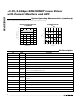
NAME FUNCTION
1, 4, 7 V
CC
1
Power Supply for Digital Circuits
2 DATA+ Noninverting PECL Input
PIN
3 DATA- Inverting PECL Input
8 LATCH TTL/CMOS Latch Input. High for latched data, low for direct data. Internal 100kΩ pull-up to V
CC
.
6 CLK- Negative PECL Clock Input. Leave unconnected if latch function is not used.
5 CLK+ Positive PECL Clock Input. Connect to V
CC
if latch function is not used.
14 APCFILT Connect a capacitor (C
APCFILT
= 0.1µF) from this pad to ground to filter the APC noise.
12 MODMON
Modulation Current Monitor. Sink current source that is proportional to the laser modulation
current.
11 BIASMON Bias Current Monitor. Sink current source that is proportional to the laser bias current.
10, 15 GND1 Ground for Digital Circuits
9 ENABLE
TTL/CMOS Enable Input. High for normal operation, low to disable laser bias and modulation
current. Internal 100kΩ pull-up to V
CC
.
19 OUT+ Positive Modulation-Current Output. I
MOD
flows through this pad when input data is high.
16, 18, 21 V
CC4
Power Supply for Output Circuitry
17 BIAS Laser Bias Current Output
13
FAIL
TTL/CMOS Failure Output. Indicates APC failure when low.
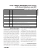
0.
5
15
10
20
25
52010 30 40 50 60
PULSE-WIDTH DISTORTION
vs. I
MOD
MAX3869-13
I
MOD
(mA)
PWD (ps)
V
CC
= +5V
V
CC
= +3.3V
0
5
10
15
20
25
30
35
40
-40 -15 10 35 60 85
MODULATION-CURRENT MONITOR GAIN
vs. TEMPERATURE
MAX3869-12
TEMPERATURE (°C)
GAIN (I
MOD
/I
MODMON
)
I
BIAS
= 100mA, I
MOD
= 50mA
I
BIAS
= 10mA, I
MOD
= 10mA