
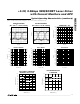
Datasheet


Optional Data Input Latch
To minimize input data pattern-dependent jitter, the dif-
ferential clock signal should be connected to the data
input latch, which is selected by an external LATCH
control. If LATCH is high, the input data is retimed by
the rising edge of CLK+. If LATCH is low, the input data
is directly connected to the output stage. When this
latch function is not used, connect CLK+ to V
CC
and
leave CLK- unconnected.
Enable Control
The MAX3869 incorporates a laser driver enable func-
tion. When ENABLE is low, both the bias and modulation
currents are off. The typical laser enable time is 250ns,
and the typical disable time is 25ns.
Current Monitors
The MAX3869 features bias- and modulation-current
monitor outputs. The BIASMON output sinks a current
equal to 1/37 of the laser bias current (I
BIAS
/ 37). The
MODMON output sinks a current equal to 1/29 of the
laser modulation current (I
MOD
/ 29). BIASMON and
MODMON should be connected through a pull-up resis-
tor to V
CC
. Choose a pull-up resistor value that ensures a
voltage at BIASMON greater than V
CC
- 1.6V and a volt-
age at MODMON greater than V
CC
- 1.0V.
Slow-Start
For laser safety reasons, the MAX3869 incorporates a
slow-start circuit that provides a delay of 250ns for
enabling a laser diode.
APC Failure Monitor
The MAX3869 provides an APC failure monitor
(TTL/CMOS) to indicate an APC loop tracking failure.
FAIL is set low when the APC loop can no longer adjust
the bias current to maintain the desired monitor current.
Short-Circuit Protection
The MAX3869 provides short-circuit protection for the
modulation, bias, and monitor current sources. If either
BIASMAX, MODSET, or APCSET is shorted to ground,
the bias and modulation output will be turned off.
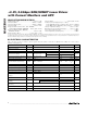
Design Procedure
When designing a laser transmitter, the optical output is
usually expressed in terms of average power and extinc-
tion ratio. Table 1 gives the relationships that are helpful
in converting between the optical average power and the
modulation current. These relationships are valid if the
mark density and duty cycle of the optical waveform are
50%.
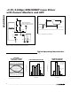
Programming the Modulation Current
For a given laser power P
AVG
, slope efficiency (η), and
extinction ration (r
e)
, the modulation current can be cal-
culated using Table 1. See the I
MOD
vs. R
MODSET
graph
in the Typical Operating Characteristics and select the
value of R
MODSET
that corresponds to the required cur-
rent at +25°C.
Programming the Bias Current
When using the MAX3869 in open-loop operation, the
bias current is determined by the R
BIASMAX
resistor. To
select this resistor, determine the required bias current
at +25°C. See the I
BIASMAX
vs. R
BIASMAX
graph in the
Typical Operating Characteristics and select the value
of R
BIASMAX
that corresponds to the required current at
+25°C.
When using the MAX3869 in closed-loop operation, the
R
BIASMAX
resistor sets the maximum bias current avail-
able to the laser diode over temperature and life. The
APC loop can subtract from this maximum value but
cannot add to it. See the I
BIASMAX
vs. R
BIASMAX
graph
in the Typical Operating Characteristics and select the
value of R
BIASMAX
that corresponds to the end-of-life
bias current at +85°C.
Programming the APC Loop
When the MAX3869’s APC feature is used, program the
average optical power by adjusting the APCSET resistor.
To select this resistor, determine the desired monitor cur-
rent to be maintained over temperature and life. See the
I
MD
vs. R
APCSET
graph in the Typical Operating
Characteristics and select the value of R
APCSET
that cor-
responds to the required current.
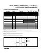
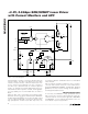
Interfacing with Laser Diodes
To minimize optical output aberrations caused by signal
reflections at the electrical interface to the laser diode, a
series damping resistor (R
D
) is required (Figure 4).
Additionally, the MAX3869 outputs are optimized for a
25Ω load. Therefore, the series combination of R
D
and
R
L
(where R
L
represents the laser-diode resistance)
MAX3869
+3.3V, 2.5Gbps SDH/SONET Laser Driver
with Current Monitors and APC
_______________________________________________________________________________________ 9
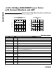
PARAMETER SYMBOL RELATION
Average Power P
AVG
P
AVG
= (P
0
+ P
1
) / 2
Extinction Ratio r
e
r
e
= P
1
/ P
0
Optical Power High P
1
P
1
= 2P
AVG
· r
e
/ (r
e
+ 1)
Optical Power Low P
0
P
0
= 2P
AVG
/ (r
e
+ 1)
Optical Amplitude Pp-p Pp-p = 2P
AVG
(r
e
- 1) / (r
e
+ 1)
Laser Slope
Efficiency
η
η = Pp-p / I
MOD
Modulation Current I
MOD
I
MOD
= Pp-p / η
Table 1. Optical Power Definition