
Datasheet
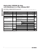


MAX44265
Chip Information
PROCESS: BiCMOS
Power-Supply Considerations
The IC is optimized for single 1.8V to 5.5V supply oper-
ation. A high amplifier power-supply rejection ratio of
95dB (typ) allows the devices to be powered directly
from a battery, simplifying design and extending bat-
tery life.
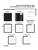
Power-Up Settling Time
The IC typically requires 5µs after power-up. Supply
settling time depends on the supply voltage, the value
of the bypass capacitor, the output impedance of the
incoming supply, and any lead resistance or induc-
tance between components. Op-amp settling time
depends primarily on the output voltage and is slew-
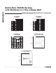
rate limited. Figure 3 shows MAX44265 in a noninvert-
ing voltage follower configuration with the input held at
midsupply. The output settles in approximately 18µs for
V
DD
= 3V (see the
Typical Operating Characteristics
for
power-up settling time).
Shutdown Mode
The IC features an active-low shutdown input. The
device enters shutdown in 2µs (typ) and exit in 30µs
(typ). The amplifier’s outputs are in a high-impedance
state in shutdown mode. Drive SHDN low to enter shut-
down. Drive SHDN high to enable the amplifier.
Power-Supply Bypassing and Layout
To minimize noise, bypass V
DD
with a 0.1µF capacitor
to ground, as close to the pin as possible.
Good layout techniques optimize performance
by decreasing the amount of stray capacitance and
inductance to the op amps’ inputs and outputs.
Minimize stray capacitance and inductance by placing
external components close to the IC.
Figure 3. Power-Up Test Configuration
MAX44265
100kΩ
100kΩ
OUT
IN-
IN+
0V
5.5V
V
DD
V
SS
Rail-to-Rail, 200kHz Op Amp
with Shutdown in a Tiny, 6-Bump WLP
______________________________________________________________________________________ 11