
Datasheet

MAX44265
Rail-to-Rail, 200kHz Op Amp
with Shutdown in a Tiny, 6-Bump WLP
2 _______________________________________________________________________________________
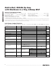
ABSOLUTE MAXIMUM RATINGS
Stresses beyond those listed under “Absolute Maximum Ratings” may cause permanent damage to the device. These are stress ratings only, and functional
operation of the device at these or any other conditions beyond those indicated in the operational sections of the specifications is not implied. Exposure to
absolute maximum rating conditions for extended periods may affect device reliability.
Power-Supply Voltage (V
DD
to V
SS
) ......................-0.3V to +6.0V
IN_+, IN_-, OUT_, SHDN_............... (V
SS
- 0.3V) to (V
DD
+ 0.3V)
Current into IN_+, IN_- ......................................................±20mA
Output Short-Circuit Duration to V
DD
or V
SS
..............Continuous
Continuous Power Dissipation (T
A
= +70°C)
6-Bump WLP (derate 10.5mW/°C above +70°C).........840mW
Operating Temperature Range .......................... -40°C to +85°C
Junction Temperature .....................................................+150°C
Storage Temperature Range ............................-65°C to +150°C
Soldering Temperature (reflow) .......................................+260°C
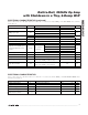
ELECTRICAL CHARACTERISTICS
(V
DD
= 1.8V to 5.5V, V
SS
= 0V, V
CM
= 0V, V
OUT
= V
DD
/2, R
L
= ∞ connected to V
DD
/2, SHDN_ = V
DD
, T
A
= +25°C, unless otherwise
noted.) (Note 1)
PARAMETER SYMBOL CONDITIONS MIN TYP MAX UNITS
Supply Voltage Range V
DD
Guaranteed by PSRR test 1.8 5.5 V
V
DD
= 1.8V 4
Supply Current I
DD
V
DD
= 5.5V 4 5.0
µA
Shutdown Supply Current I
DD
(
SHDN_
)
SHDN_ = GND 0.001 0.5 µA
Input Offset Voltage V
OS
±0.2 ±1mV
Input Bias Current I
B
(Note 2) ±1 ±10 pA
Input Offset Current I
OS
(Note 2) ±1 ±10 pA
Common mode 1
Input Resistance R
IN
Differential mode, -1mV < V
IN
< +1mV 10
GΩ
Input Common-Mode Range V
CM
Guaranteed by CMRR test
V
SS
-
0.1
V
DD
+
0.1
V
Common-Mode Rejection Ratio CMRR -0.1V < V
CM
< V
DD
+ 0.1V, V
DD
= 5.5V 70 80 dB
Power-Supply Rejection Ratio PSRR 1.8V < V
DD
< 5.5V 65 95 dB
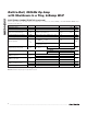
25mV < V
OUT
< V
DD
- 25mV,
R
L
= 100kΩ, V
DD
= 5.5V
95 120
Open-Loop Gain A
VOL
100mV < V
OUT
< V
DD
- 100mV,
R
L
= 5kΩ, V
DD
= 5.5V
95 110
dB
R
L
= 100kΩ 2.5 5
R
L
= 5kΩ 50 70Output-Voltage-Swing High V
OH
V
DD
- V
OUT
R
L
= 1kΩ 250
mV
R
L
= 100kΩ 2.5 5
R
L
= 5kΩ 50 70
Output-Voltage-Swing Low V
OL
V
OUT
- V
SS
R
L
= 1kΩ 250
mV
Output Short-Circuit Current I
OUT(SC)
±15 mA