
Datasheet


MAX4810/MAX4811/MAX4812
Dual, Unipolar/Bipolar, High-Voltage
Digital Pulsers
2 _______________________________________________________________________________________
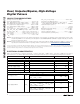
ABSOLUTE MAXIMUM RATINGS
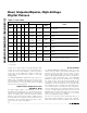
ELECTRICAL CHARACTERISTICS
(V
DD
= +2.7V to +6V, V
CC_
= +4.75V to +12.6V, V
EE_
= -12.6V to -4.75V, V
NN_
= -200V to 0, V
PP_
= 0 to (V
NN_
+ 200V), V
SS
≤ the lower of
V
NN1
or V
NN2
, T
A
= T
J
= T
MIN
to T
MAX
, unless otherwise noted. Typical values are at T
A
= +25°C.) (Note 3) (See Figures 8, 9, and 10.)
Stresses beyond those listed under “Absolute Maximum Ratings” may cause permanent damage to the device. These are stress ratings only, and functional
operation of the device at these or any other conditions beyond those indicated in the operational sections of the specifications is not implied. Exposure to
absolute maximum rating conditions for extended periods may affect device reliability.
(Voltages referenced to GND.)
V
DD
Logic Supply Voltage........................................-0.3V to +6V
V
CC_
Output Driver Positive Supply Voltage ..........-0.3V to +15V
V
EE_
Output Driver Negative Supply Voltage.........-15V to +0.3V
V
PP_
High Positive Supply Voltage.......................-0.3V to +230V
V
NN_
High Negative Supply Voltage ....................-230V to +0.3V
V
SS
Voltage................................................(V
PP_
- 250V) to V
NN_
V
PP1
- V
NN1
, V
PP2
- V
NN2
Supply Voltage............-0.6V to +250V
INP_, INN_, INC_, EN_, SHDN Logic Input...-0.3V to V
DD
+ 0.3V
O
P_,
O
CP_
, O
LN_
, O
N_
..............(-0.3V + V
NN_
) to (-0.3V to V
PP_
)
C
GN_
Voltage............................(-0.3V + V
NN_
) to (+15V + V
NN_
)
C
GP_
Voltage .............................(+0.3V + V
PP_
) to (-15V + V
PP_
)
C
GC_
Voltage...........................................................-15V to +15V
C
DC_,
C
DP_
, C
DN_
Voltage......................................-0.3V to V
CC_
Peak Current per Output Channel ........................................3.0A
Continuous Power Dissipation (T
A
= +70°C) (Note 1)
56-Pin TQFN (derate 40mW/°C above +70°C) ..........3200mW
Thermal Resistance (Note 2)
θ
JA
................................................................................25°C/W
θ
JC
...............................................................................0.8°C/W
Operating Temperature Range...............................0°C to +70°C
Junction Temperature......................................................+150°C
Storage Temperature Range .............................-65°C to +150°C
Lead Temperature (soldering, 10s) .................................+300°C
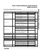
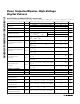
PARAMETER
SYMBOL
CONDITIONS
MIN TYP MAX UNITS
POWER SUPPLY (V
DD
, V
CC_
, V
EE
_, V
PP_
, V
NN_
)
Logic Supply Voltage V
DD
+2.7
+3 +6 V
Positive Drive Supply Voltage V
CC_
+4.75 +12 +12.6
V
Negative Drive Supply Voltage
V
EE_
-12.6
-12
-4.75
V
High-Side Supply Voltage V
PP_
0
V
NN_
+
220
V
Low-Side Supply Voltage V
NN_
-200
0V
V
PP_
- V
NN_
Supply Voltage 0
+220
V
SUPPLY CURRENT (Single Channel)
V
INN_
/V
INP_
= 0
, V
SHDN
= 0 1
V
DD
Supply Current I
DD
V
EN_
= V
DD
, V
SHDN
= V
DD
, V
INC_
= 0 or V
DD
,
V
INN_
= V
INP_
, f = 5MHz
100 200
µA
V
SHDN
= 0, CH1 and CH2 1
V
EN_
= V
DD
, V
SHDN
= V
DD,
CH1 and CH2
130 200
µA
V
EN_
= V
DD
, V
SHDN
= V
DD
, V
INC_
= 0 or V
DD
,
V
INN_
= V
INP_
, f = 5MHz, V
CC_
= 5V, V
DD
= 3V,
only one channel switching
15
V
CC_
Supply Current I
CC_
V
EN_
= V
DD
, V
SHDN
= V
DD
, V
INC_
= 0 or V
DD
,
V
INN_
= V
INP_
, f = 5MHz, V
CC_
= 12V, V
DD
= 3V,
only one channel switching
36
mA
Note 1: This specification is based on the thermal characteristic of the package, the maximum junction temperature, and the setup
described by JEDEC 51. The maximum power dissipation for the MAX4810/MAX4811/MAX4812 might be limited by the thermal
protection included in the device.
Note 2: Package thermal resistances were obtained using the method described in JEDEC specification JESD51-7, using a four-
layer board. For detailed information on package thermal considerations, refer to www.maxim-ic.com/thermal-tutorial
.