
Datasheet


MAX4810/MAX4811/MAX4812
Dual, Unipolar/Bipolar, High-Voltage
Digital Pulsers
10 ______________________________________________________________________________________
controls the on and off states of the high side FET, INN_
controls the on and off states of the low side FET, INC_
controls the active clamp and EN_ controls the gate to
source short. These signals give complete control of the
output stage of each driver (see Table 1 for all logic
combinations).
The MAX4810/MAX4811/MAX4812 logic inputs are
CMOS logic compatible and the logic level are refer-
enced to V
DD
for maximum flexibility. The low 5pF (typ)
input capacitance of the logic inputs reduces loading
and increases switching speed.
High-Voltage Output Protection
(MAX4811 Only)
The high-voltage outputs of the MAX4811 feature an
integrated overvoltage protection circuit that allows the
user to implement multilevel pulsing by connecting the
outputs of multiple pulser channels in parallel. Internal
diodes in series with the ON_ and OP_ outputs prevent
the body diode of the high-side and low-side FETs from
switching on when a voltage greater than V
NN_
or V
PP_
is present on the output. See Figure 2.
Active Clamps
The MAX4810/MAX4811/MAX4812 feature an active
clamp circuit to improve pulse quality and reduce 2nd
harmonic output. The clamp circuit consists of an N-
channel (DC-coupled) and a P-channel (AC and DC
delay coupled) high-voltage FETs that are switched on
or off by the logic clamp input (INC_). The MAX4810/
MAX4811 feature protected clamp devices, allowing
the clamp circuit to be used in bipolar pulsing circuits
(see Figures 1 and 2). A diode in series with the OCN_
output prevents the body diode of the low-side FET
from turning on when a voltage lower than GND is pre-
sent. Another diode in series with the OCP_ output pre-
vents the body diode of the high-side FET from turning
on when a voltage higher than ground is present. The
MAX4812 does not have diode protection on the clamp
outputs. Thus, the device is suitable for use in circuits
where only unipolar pulsing is required.
The user can connect the active clamp input (INC_) to a
logic-high voltage and drive only the INP_ and INN_
inputs to minimize the number of signals used to drive the
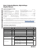
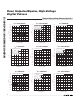
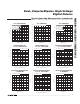
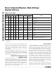
X = Don’t care.
0 = Logic-low.
1 = Logic-high.
INPUTS OUTPUTS
SDHN
EN_ INP_ INN_ INC_
OP_ ON_
OCP_,
OCN_
STATE
0XX
X
0
High
impedance
High
impedance
High
impedance
Powered down, INP_/INN_ disabled, gate-source
short disabled
0XX
X
1
High
impedance
High
impedance
GND
Powered down, INP_/INN_ disabled, gate-source
short disabled
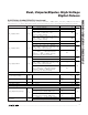
10X
X
0
High
impedance
High
impedance
High
impedance
Powered up, INP_/INN_ disabled, gate-source short
enabled
10X
X
1
High
impedance
High
impedance
GND
Powered up, INP_/INN_ disabled, gate-source short
enabled
1 1000
High
impedance
High
impedance
High
impedance
Powered up, all inputs enabled, gate-source short
disabled
1 1001
High
impedance
High
impedance
GND
Powered up, all inputs enabled, gate-source short
disabled
1 101X
High
impedance
V
NN_
High
impedance
Powered up, all inputs enabled, gate-source short
disabled
1 110X
V
PP_
High
impedance
High
impedance
Powered up, all inputs enabled, gate-source short
disabled
1 111X
V
PP_
V
NN_
High
impedance
Not allowed (3ns maximum overlap)
Table 1. Truth Table