
Datasheet


MAX4810/MAX4811/MAX4812
Dual, Unipolar/Bipolar, High-Voltage
Digital Pulsers
8 _______________________________________________________________________________________
Pin Description
PIN NAME FUNCTION
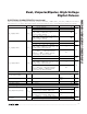
1
C
GP1
Channel 1 High-Side Gate Input. Connect a 1nF to 10nF capacitor between C
DP1
and C
GP1
as close as
possible to the device.
2 , 3
V
PP1
Channel 1 High-Side Positive Supply Voltage Input. Bypass V
PP1
to GND with a 0.1µF as close as
possible to the device. See the
Power Supplies and Bypassing
section. Depending on the output,
additional bypassing may be required.
4, 10, 33,
39
N.C. No Connection. Not connected internally.
5 OP1 Channel 1 High-Side Drain Output
6 OCP1 Channel 1 High-Side Clamp Output
7, 15, 28,
36, 44, 55
GND Ground
8 OCN1 Channel 1 Low-Side Clamp Output
9 ON1 Channel 1 Low-Side Drain Output
11, 12
V
NN1
Channel 1 High-Side Negative Supply Voltage Input. Bypass V
NN1
to GND with a 0.1µF as close as
possible to the device. See the
Power Supplies and Bypassing
section. Depending on the output,
additional bypassing may be required.
13
C
GN1
Channel 1 Low-Side Gate Input. Connect a 1nF to 10nF capacitor between C
DN1
and C
GN1
as close as
possible to the device.
14
C
DN1
Channel 1 Low-Side Driver Output. Connect a 1nF to 10nF capacitor between C
DN1
and C
GN1
as close
as possible to the device.
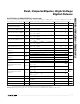
16, 54
V
CC1
Channel 1 Gate-Drive Supply Voltage Input. Bypass V
CC1
to GND with a 0.1µF as close as possible to
the device. See the
Power Supplies and Bypassing
section. Depending on the output, additional
bypassing may be required.
17 INN1 Channel 1 Low-Side Logic Input (Table 1)
18 INC1
Channel 1 Clamp Logic Input. Clamps OCP1 and OCN1 are turned on when INC1 is high and when INP1
and INN1 are low (see Table 1).
19 INP1 Channel 1 High-Side Logic Input (Table 1)
20 EN1
Channel 1 Enable Logic Input. Drive EN1 high to enable OP1 and ON1. Pull EN1 low to turn on the gate-
source short circuit (see Table 1).
21
SHDN
Shutdown Logic Input (Table 1)
22 AGND Analog Ground. Must be connected to common GND.
23 EN2
Channel 2 Enable Logic Input. Drive EN2 high to enable OP2 and ON2. Pull EN2 low to turn on the gate-
source short circuit. See Table 1.
24 INP2 Channel 2 High-Side Logic Input (Table 1)
25 INC2
Channel 2 Clamp Logic Input. Clamps OCP2 and OCN2 are turned on when INC2 is high and when INP2
and INN2 are low. See Table 1.
26 INN2 Channel 2 Low-Side Logic Input (Table 1)
27, 45
V
CC2
Channel 2 Gate-Drive Supply Voltage Input. Bypass V
CC2
to GND with a 0.1µF as close as possible to
the device. See the
Power Supplies and Bypassing
section. Depending on the output, additional
bypassing may be required.
29
C
DN2
Channel 2 Low-Side Driver Output. Connect a 1nF to 10nF capacitor between C
DN2
and C
GN2
as close
as possible to the device.
30
C
GN2
Channel 2 Low-Side Gate Input. Connect a 1nF to 10nF capacitor between C
DN2
and C
GN2
as close as
possible to the device.