
Datasheet

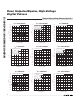
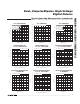

MAX4810/MAX4811/MAX4812
Dual, Unipolar/Bipolar, High-Voltage
Digital Pulsers
_______________________________________________________________________________________ 9
Detailed Description
The MAX4810/MAX4811/MAX4812 are dual high-volt-
age, high-speed pulsers that can be independently
configured for either unipolar or bipolar pulse outputs.
These devices have independent logic inputs for full
pulse control and independent active clamps. The
clamp input, INC_, can be set high to activate the
clamp automatically when the device is not pulsing to
the positive or negative high-voltage supplies.
Logic Inputs (INP_, INN_, INC_, EN_,
SHDN
)
The MAX4810/MAX4811/MAX4812 have a total of nine
logic input signals. SHDN controls power-up and power-
down of the device. There are two sets of INP_, INN_,
INC_, and EN_ signals: one for each channel. INP_
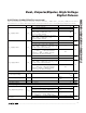
PIN NAME FUNCTION
31, 32
V
NN2
Channel 2 High-Side Negative Supply Voltage Input. Bypass V
NN2
to GND with a 0.1µF as close as
possible to the device. See the
Power Supplies and Bypassing
section. Depending on the output,
additional bypassing may be required.
34 ON2 Channel 2 Low-Side Drain Output
35 OCN2 Channel 2 Low-Side Clamp Output
37 OCP2 Channel 2 High-Side Clamp Output
38 OP2 Channel 2 High-Side Drain Output
40, 41
V
PP2
Channel 2 High-Side Supply Voltage Input. Bypass V
PP2
to GND with a 0.1µF as close as possible to the
device. See the
Power Supplies and Bypassing
section. Depending on the output, additional bypassing
may be required.
42
C
GP2
Channel 2 High-Side Gate Input. Connect a 1nF to 10nF capacitor between C
DP2
and C
GP2
as close as
possible to the device.
43
C
DP2
Channel 2 High-Side Driver Output. Connect a 1nF to 10nF capacitor between C
DP2
and C
GP2
as close
as possible to the device.
46
C
GC2
Channel 2 High-Side Clamp Gate Input. Connect a 1nF to 10nF capacitor between C
DC2
and C
GC2
as
close as possible to the device.
47
C
DC2
Channel 2 High-Side Clamp Driver Output. Connect a 1nF to 10nF capacitor between C
DC2
and C
GC2
as
close as possible to the device.
48
V
EE2
Channel 2 Negative Supply Input. |V
EE2
|
≤
V
CC2
. Gate Drive Supply Voltage for the OCP clamp. Bypass
V
EE2
to GND with a 0.1µF as close as possible to the device. See the
Power Supplies and Bypassing
section. Depending on the output, additional bypassing may be required.
49
V
DD
Logic Supply Voltage Input. Bypass V
DD
to GND with a 0.1µF as close as possible to the device. See the
Power Supplies and Bypassing
section. Depending on the output, additional bypassing may be
required.
50
V
SS
Substrate Voltage. Connect V
SS
to a voltage equal to or more negative than the more negative of V
NN1
or
V
NN2
.
51
V
EE1
Channel 1 Negative Supply Input. |V
EE1
|
≤
V
CC1
. Gate Drive Supply Voltage for the OCP clamp. Bypass
V
EE1
to GND with a 0.1µF as close as possible to the device. See the
Power Supplies and Bypassing
section. Depending on the output, additional bypassing may be required.
52
C
DC1
Channel 1 High-Side Clamp Driver Output. Connect a 1nF to 10nF capacitor between C
DC1
and C
GC1
as
close as possible to the device.
53
C
GC1
Channel 1 High-Side Clamp Gate Input. Connect a 1nF to 10nF capacitor between C
DC1
and C
GC1
as
close as possible to the device.
56
C
DP1
Channel 1 High-Side Driver Output. Connect a 1nF to 10nF capacitor between C
DP1
and C
GP1
as close
as possible to the device.
—EP
Exposed Pad. EP must be connected to V
SS
. Do not use EP as the only V
SS
connection for the device.
Pin Description (continued)