
Datasheet
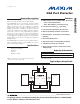


MAX4895E
VGA Port Protector
2 _______________________________________________________________________________________
ABSOLUTE MAXIMUM RATINGS
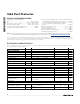
ELECTRICAL CHARACTERISTICS
(V
CC
= +4.5V to +5.5V, V
L
= +2.0V to V
CC
, T
A
= T
MIN
to T
MAX
, unless otherwise noted. Typical values are at V
CC
= +5.0V,
V
L
= +3.3V, and T
A
= +25°C.) (Note 2)
Stresses beyond those listed under “Absolute Maximum Ratings” may cause permanent damage to the device. These are stress ratings only, and functional
operation of the device at these or any other conditions beyond those indicated in the operational sections of the specifications is not implied. Exposure to
absolute maximum rating conditions for extended periods may affect device reliability.
Note 1: Package thermal resistances were obtained using the method described in JEDEC specification JESD51-7, using a four-
layer board. For detailed information on package thermal considerations, refer to www.maxim-ic.com/thermal-tutorial
.
(All voltages referenced to GND.)
V
CC
........................................................................-0.3V to +6.0V
V
L
.............................................................-0.3V to +(V
CC
+ 0.3V)
R, G, B, H1, V1, SCL1, SDA1...................-0.3V to +(V
CC
+ 0.3V)
EN, H0, V0, SCL0, SDA0 ............................-0.3V to +(V
L
+ 0.3V)
Continuous Current through SDA_, SCL_.........................±30mA
Continuous Short-Circuit Current H1, V1..........................±20mA
Continuous Power Dissipation (T
A
= +70°C) for multilayer board:
16-Pin TQFN (derate 20.8mW/°C above +70°C) .......1667mW
Junction-to-Case Thermal Resistance (θ
JC
) (Note 1) ......7°C/W
Junction-to-Ambient Thermal Resistance (θ
JA
)
(Note 1) ........................................................................48°C/W
Operating Temperature Range ...........................-40°C to +85°C
Junction Temperature......................................................+150°C
Storage Temperature Range .............................-65°C to +150°C
Lead Temperature (soldering, 10s) .................................+300°C
Soldering Temperature (reflow) .......................................+260°C
PARAMETER SYMBOL CONDITIONS MIN TYP MAX UNITS
SUPPLY OPERATION
Supply Voltage V
CC
4.5 5.5 V
Logic Supply Voltage V
L
V
L
V
CC
2 3.3 5.5 V
V
CC
Supply Current I
CC
V
H0
, V
V0
= 0V, V
EN
= V
L
0.5 5.0 μA
V
L
Supply Current I
L
V
H0
, V
V0
= 0V, V
EN
= V
L
(no load) 0.5 5.0 μA
RGB CHANNELS
R, G, B Capacitance C
OUT
f = 1MHz, V
R,G,B
= 1V
P-P
(Note 3) 2.2 pF
R, G, B Leakage V
CC
= +5.5V -1 +1 μA
H_, V_, EN CHANNELS
Input Threshold Low V
IL
V
L
= +3.0V 0.8 V
Input Threshold High V
IH
V
L
= +3.6V 2.0 V
Input Hysteresis V
HYST
100 mV
Input Leakage Current I
LEAK
V
L
= +3.3V, V
CC
= +5.5V -1 +1 μA
Output-Voltage Low V
OL
I
OUT
= 10mA sink, V
CC
= +4.5V 0.8 V
Output-Voltage High V
OH
I
OUT
= 10mA source, V
CC
= +4.5V 2.4 V
Propagation Delay t
PD
R
L
= 2.2k, C
L
= 10pF, V
OL
= +0.8V,
V
OH
= +2.4V
15 ns
Enable Time t
ON
, t
OFF
15 ns
SDA_, SCL_ (DDC) CHANNELS
On-Resistance, SDA, SCL R
ON
V
CC
= +5.5V, I
SDA, SCL
= ±10mA,
V
SDA, SCL
= +0.5V
20 55
Leakage Current, SDA, SCL I
LEAK
V
L
= 0V -1 +1 μA