
Datasheet
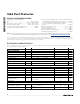


MAX4895E
VGA Port Protector
_______________________________________________________________________________________ 5
Applications Information
The MAX4895E provides the level shifting necessary to
drive two standard VGA ports from a graphics controller
as low as +2.2V. Internal buffers drive the HSYNC and
VSYNC signals to VGA standard TTL levels. The DDC
switch provides level shifting by clamping signals to a
diode drop less than V
L
(see the
Typical Operating
Circuit
). Connect V
L
to +3.3V for normal operation.
Power-Supply Decoupling
Bypass V
CC
and V
L
to ground with a 1µF ceramic
capacitor as close as possible to the device.
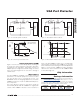
PCB Layout
High-speed switches such as the MAX4895E require
proper PCB layout for optimum performance. Ensure
that impedance-controlled PCB traces for high-speed
signals are matched in length and are as short as pos-
sible. Connect the exposed pad to a solid ground
plane.
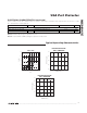
Functional Diagram
MAX4895E
±15kV±15kV±15kV
H1
V1
H0
V0
EN
SCL0
SDA1
SCL1
SDA0
CLAMP
±15kV±15kV
B
±15kV
G
±15kV
R
V
L
V
CC
GND