
Datasheet
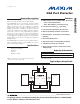


MAX4895E
VGA Port Protector
6 _______________________________________________________________________________________
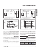
Detailed Description
The MAX4895E integrates level-translating buffers and
features R, G, B port protection for VGA signals.
Horizontal and vertical synchronization (H0/V0) inputs
feature level-shifting buffers to support low-voltage
CMOS or standard TTL-compatible graphics con-
trollers. The device meets ±10mA VESA drive require-
ments. The MAX4895E also features I
2
C level shifting
using two nMOS devices. All outputs maintain ±15kV
Human Body Model (HBM) and ±8kV Contact
Discharge per IEC 61000-4-2 on seven terminals
(SDA1, SCL1, H1, V1, R, G, B). The R, G, B pads pro-
tect the digital-to-analog converter (DAC) and are sim-
ply placed in parallel with the R, G, B outputs for the
DAC and VGA socket.
Horizontal/Vertical Sync Level Shifter
HSYNC/VSYNC are buffered to provide level shifting
and drive capability to meet the VESA specification.
Input logic levels (V
IL
, V
IH
) are connected to V
L
(see
the
Electrical Characteristics
table). The level-shifted
outputs (H1 and V1) are pulled low when EN is driven
low (see Table 1). Logic-level output (V
OL
, V
OH
) are
+5.0V TTL compatible.
Display Data Channel Switches
The MAX4895E incorporates two nMOS switches for I
2
C
level shifting. The SDA, SCL terminals are voltage
clamped to a diode drop less than the V
L
voltage.
Voltage clamping provides protection and compatibility
with SDA, SCL signals and low-voltage ASICs. Supply
+2.5V to +3.3V on V
L
to provide voltage clamping for
VESA I
2
C-compatible signals. The SDA, SCL switches
are identical, and each switch can be used to route
SDA or SCL signals.
RGB
There are three terminals for R, G, and B. The only
function of these terminals is to provide high-level ESD
protection to the RGB lines, while at the same time,
keeping the capacitance on the RGB lines to a mini-
mum. The R, G, B terminals are identical, and any of
the three terminals can be used to protect red, green,
or blue video signals.
ESD Protection
As with all Maxim devices, ESD-protection structures
are incorporated on all terminals to protect against
electrostatic discharges encountered during handling
and assembly. Additionally, the MAX4895E is protected
to ±15kV on the RGB terminals and outputs H1, V1,
SDA1, and SCL1 by the Human Body Model (HBM). For
optimum ESD performance, bypass V
CC
to ground with
a 1µF ceramic capacitor.
ESD protection can be tested in various ways. The R,
G, B terminals and outputs H1, V1, SDA1, and SCL1 of
the MAX4895E are characterized for protection to the
following limits:
• ±15kV using the Human Body Model
• ±8kV IEC 61000-4-2 Contact Discharge
ESD Test Conditions
ESD performance depends on a variety of conditions.
Contact Maxim for a reliability report documenting test
setup, methodology, and results.
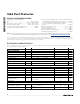
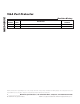
Table 1. HV Truth Table
EN FUNCTION
1 HSYNC/VSYNC level shifting enabled
0 H1, V1 = 0
Table 2. DDC Truth Table
EN FUNCTION
1
SDA0 to SDA1
SCL0 to SCL1
0 SDA1, SCL1, high impedance