
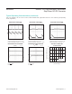
Datasheet

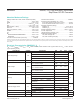
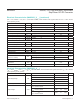
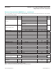


PIN NAME FUNCTION
1 BST Boost Capacitor Connection. Connect a 0.1μF ceramic capacitor from BST to LX.
2 VD Internal Regulator Output. Bypass VD to GND with a 0.1μF ceramic capacitor.
3 SGND Internal Connection. SGND must be connected to GND.
4 FB
Output Sense Feedback Connection. For xed output voltage (MAX5033A, MAX5033B, MAX5033C),
connect FB to V
OUT
. For adjustable output voltage (MAX5033D), use an external resistive voltage-
divider to set V
OUT
. V
FB
regulating set point is 1.22V.
5
ON/OFF
Shutdown Control Input. Pull ON/OFF low to put the device in shutdown mode. Drive ON/OFF high
for normal operation.
6 GND Ground.
7 V
IN
Input Voltage. Bypass V
IN
to GND with a low-ESR capacitor as close to the device as possible.
8 LX Source Connection of Internal High-Side Switch.
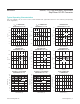
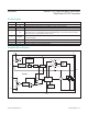
ENABLE
LX
BST
V
IN
ON/OFF
V
REF
REGULATOR
(FOR DRIVER)
REGULATOR
(FOR ANALOG)
OSC
RAMP
HIGH-SIDE
CURRENT
SENSE
I
REF-PFM
I
REF-LIM
CPFM
1.69V
CILIM
FB
x1
V
REF
EAMP
CONTROL
LOGIC
CPWM
VD
GND
R
h
R
l
CLK
SGND
MAX5033
TYPE 3
COMPENSATION
THERMAL
SHUTDOWN
RAMP
MAX5033 500mA, 76V, High-Efciency, MAXPower
Step-Down DC-DC Converter
www.maximintegrated.com
Maxim Integrated
│
8
Pin Description
Simplied Block Diagram