
Datasheet


Detailed Description
The MAX5033 step-down DC-DC converter operates
from a 7.5V to 76V input voltage range. A unique volt-
age- mode control scheme with voltage feed-forward
and an internal switching DMOS FET provides high
efficiency over a wide input voltage range. This pulse-
width modulated converter operates at a fixed 125kHz
switching frequency. The device also features automatic
pulse-skipping mode to provide low quiescent current and
high efficiency at light loads. Under no load, the MAX5033
consumes only 270μA, and in shutdown mode, consumes
only 10μA. The MAX5033 also features undervoltage
lockout, hiccup-mode output shortcircuit protection, and
thermal shutdown.
Shutdown Mode
Drive ON/OFF to ground to shut down the MAX5033.
Shutdown forces the internal power MOSFET off, turns
off all internal circuitry, and reduces the V
IN
supply cur-
rent to 10μA (typ). The ON/OFF rising threshold is 1.69V
(typ). Before any operation begins, the voltage at ON/OFF
must exceed 1.69V (typ). The ON/OFF input has 100mV
hysteresis.
Undervoltage Lockout (UVLO)
Use the ON/OFF function to program the UVLO threshold
at the input. Connect a resistive voltage-divider from V
IN
to GND with the center node to ON/OFF as shown in
Figure 1. Calculate the threshold value by using the fol-
lowing formula:
UVLO(TH)
R1
V 1 1.85V
R2
=+×
The minimum recommended V
UVLO(TH)
is 6.5V, 7.5V,
and 13V for the output voltages of 3.3V, 5V, and 12V,
respectively. The recommended value for R2 is less than
1MΩ.
If the external UVLO threshold-setting divider is not used,
an internal undervoltage-lockout feature monitors the
supply voltage at V
IN
and allows operation to start when
V
IN
rises above 5.2V (typ). This feature can be used only
when V
IN
rise time is faster than 2ms. For slower V
IN
rise
time, use the resistive divider at ON/OFF.
Boost High-Side Gate Drive (BST)
Connect a flying bootstrap capacitor between LX and
BST to provide the gate-drive voltage to the high-side
n-channel DMOS switch. The capacitor is alternately
charged from the internally regulated output-voltage
VD and placed across the high-side DMOS driver. Use
a 0.1μF, 16V ceramic capacitor located as close to the
device as possible.
On startup, an internal low-side switch connects LX to
ground and charges the BST capacitor to VD. Once the
BST capacitor is charged, the internal low-side switch is
turned off and the BST capacitor voltage provides the
necessary enhancement voltage to turn on the high-side
switch.
Thermal-Overload Protection
The MAX5033 features integrated thermal-overload pro-
tection. Thermal-overload protection limits total power dis-
sipation in the device, and protects the device in the event
of a fault condition. When the die temperature exceeds
+160°C, an internal thermal sensor signals the shutdown
logic, turning off the internal power MOSFET and allow-
ing the IC to cool. The thermal sensor turns the internal
power MOSFET back on after the IC’s die temperature
cools down to +140°C, resulting in a pulsed output under
continuous thermaloverload conditions.
Applications Information
Setting the Output Voltage
The MAX5033A/B/C have preset output voltages of 3.3V,
5.0V, and 12V, respectively. Connect FB to the preset
output voltage (see the Typical Operating Circuit).
The MAX5033D offers an adjustable output voltage. Set
the output voltage with a resistive voltage-divider connect-
ed from the circuit’s output to ground (Figure 1). Connect
the center node of the divider to FB. Choose R4 less than
15kΩ, then calculate R3 as follows:
OUT
(V 1.22)
R3 R4
1.22
−
= ×
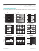
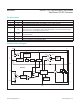
Figure 1. Adjustable Output Voltage
MAX5033D
GND
BST
LX
V
IN
SGND
FB
D1
50SQ100
VD
220µH
V
OUT
5V, 0.5A
V
IN
7.5V TO 76V
47µF
0.1µF
0.1µF
C
OUT
33µF
R1
R2
R3
41.2kΩ
R4
13.3kΩ
ON/OFF
MAX5033 500mA, 76V, High-Efciency, MAXPower
Step-Down DC-DC Converter
www.maximintegrated.com
Maxim Integrated
│
9