
Datasheet

MAX5066
Configurable, Single-/Dual-Output, Synchronous
Buck Controller for High-Current Applications
10 ______________________________________________________________________________________
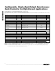
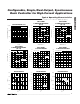
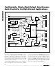
Two enable comparators (CEN1 and CEN2) are avail-
able to control and sequence the two PWM sections
through the enable (EN1 or EN2) inputs. An oscillator,
with an externally programmable frequency generates
two clock pulse trains and two ramps for both PWM
sections. The two clocks and the two ramps are 180°
out of phase with each other.
A linear regulator (REG) generates the 5V to supply the
device. This regulator has the output-current capability
necessary to provide for the MAX5066’s internal circuit-
ry and the power for the external MOSFET’s gate dri-
vers. A low-current linear regulator (REF) provides a
precise 3.3V reference output and is capable of driving
loads of up to 200µA. Internal UVLO circuitry ensures
that the MAX5066 starts up only when V
REG
and V
REF
are at the correct voltage levels to guarantee safe oper-
ation of the IC and of the power MOSFETs.
16
17
18
19
BST1
DH1
LX1
DL1
20
27
26
25
24
23
BST2
DH2
LX2
DL2
PGND
V
DD
2
CSP2
1
CSN2
13
CSP1
14
CSN1
CA1
11
EAN1
6
REF
AGND
8
EN1
15
EN2
28
CA2
CPWM1
CPWM2
7
RT/CLKIN
CEA1
CEA2
12EAOUT1
9
MODE
3
EAOUT2
5
CLP2
10
CLP1
22
IN
21
REG
1.225V
1.225V
THERMAL
SHUTDOWN
V
DD
MUX
4
EAN2
CEN1
VEA1
DF1 AND
HICCUP
LOGIC
EXTERNAL FREQUENCY SYNC
0°
CONTROL
AND DRIVER
LOGIC 1
CONTROL
AND DRIVER
LOGIC 2
DF2 AND
HICCUP
LOGIC
OSCILLATOR
AND PHASE
SPLITTER
180°
2V
P-P
RAMP
V
REG
= 5V
FOR INTERNAL
BIASING
UVLO
V
REF
= 3.3V
UV33
V
INTREF
= 0.61V
VEA2
CEN2
2V
P-P
RAMP
Figure 1. Block Diagram