
Datasheet

MAX5066
Configurable, Single-/Dual-Output, Synchronous
Buck Controller for High-Current Applications
2 _______________________________________________________________________________________
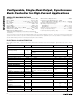
ABSOLUTE MAXIMUM RATINGS
Stresses beyond those listed under “Absolute Maximum Ratings” may cause permanent damage to the device. These are stress ratings only, and functional
operation of the device at these or any other conditions beyond those indicated in the operational sections of the specifications is not implied. Exposure to
absolute maximum rating conditions for extended periods may affect device reliability.
IN to AGND.............................................................-0.3V to +30V
BST_ to AGND........................................................-0.3V to +35V
DH_ to LX_ ....................................-0.3V to (V
BST_
- V
LX_
) + 0.3V
DL_ to PGND..............................................-0.3V to (V
DD
+ 0.3V)
BST_ to LX_ ..............................................................-0.3V to +6V
V
DD
to PGND............................................................-0.3V to +6V
AGND to PGND .....................................................-0.3V to +0.3V
REG, RT/CLKIN, CSP_, CSN_ to AGND ..................-0.3V to +6V
All Other Pins to AGND ............................-0.3V to (V
REG
+ 0.3V)
REG Continuous Output Current
(Limited by Power Dissipation, No Thermal or Short-Circuit
Protection).........................................................................67mA
REF Continuous Output Current ........................................200µA
Continuous Power Dissipation (T
A
= +70°C)
28-Pin TSSOP (derate 23.8mW/°C above +70°C) .....1904mW
Package Thermal Resistance (
θ
JC
) ...................................2°C/W
Operating Temperature Ranges
MAX5066EUI ...................................................-40°C to +85°C
MAX5066AUI .................................................-40°C to +125°C
Maximum Junction Temperature .....................................+150°C
Storage Temperature Range .............................-60°C to +150°C
Lead Temperature (soldering, 10s) .................................+300°C
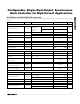
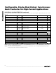
ELECTRICAL CHARACTERISTICS
(V
IN
= V
REG
= V
DD
= V
EN_
= +5V, T
A
= T
J
= T
MIN
to T
MAX
, unless otherwise noted, circuit of Figure 6. Typical values are at T
A
= +25°C.)
(Note 1)
PARAMETER
SYMBOL
CONDITIONS
MIN TYP MAX
UNITS
SYSTEM SPECIFICATIONS
528
Input Voltage Range V
IN
IN and REG shorted together for +5V
operation
4.75
5.5
V
Quiescent Supply Current I
IN
f
OSC
= 500kHz, DH_, DL_ = open 4 20 mA
STARTUP/INTERNAL REGULATOR OUTPUT (REG)
REG Undervoltage Lockout UVLO V
REG
rising 4.0
4.15
4.5 V
Hysteresis V
HYST
200
mV
REG Output Accuracy V
IN
= 5.8V to 28V, I
SOURCE
= 0 to 65mA
4.75 5.10 5.30
V
REG Dropout V
IN
< 5.8V, I
SOURCE
= 60mA 0.5 V
INTERNAL REFERENCE
Internal Reference Voltage V
EAN_
EAN_ connected to EAOUT_ (Note 2)
0.6135
V
Internal Reference Voltage
Accuracy
V
EAN_
V
IN
= V
REG
= 4.75V to 5.5V or V
IN
= 5V to
28V, EAN_ connected to EAOUT_ (Note 2)
-0.9 +0.9
%
EXTERNAL REFERENCE VOLTAGE OUTPUT (REF)
Accuracy V
REF
I
REF
= 100µA
3.23
3.3
3.37
V
Load Regulation I
REF
= 0 to 200µA 3.2 3.4 V
MOSFET DRIVERS
p-Channel Output Driver
Impedance
R
ON_P
1.35
4 Ω
n-Channel Output Driver
Impedance
R
ON_N
0.45 1.35
Ω
Output Driver Source Current
I
DH_
, I
DL_
2.5 A
Output Driver Sink Current
I
DH_
, I
DL_
8A
Nonoverlap Time (Dead Time) t
NO
C
DH_
or C
DL_
= 5nF 30 ns