
Datasheet

MAX5066
Configurable, Single-/Dual-Output, Synchronous
Buck Controller for High-Current Applications
8 _______________________________________________________________________________________
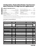
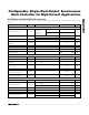
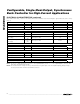
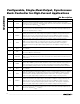
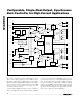
Pin Description
PIN NAME FUNCTION
1 CSN2
Current-Sense Differential Amplifier Negative Input for Output2. Connect CSN2 to the negative
terminal of the sense resistor. The differential voltage between CSP2 and CSN2 is internally amplified
by the current-sense amplifier (A
V(CS)
= 36V/V).
2 CSP2
Current-Sense Differential Amplifier Positive Input for Output2. Connect CSP2 to the positive terminal
of the sense resistor. The differential voltage between CSP2 and CSN2 is internally amplified by the
current-sense amplifier (A
V(CS)
= 36V/V).
3 EAOUT2
Voltage Error-Amplifier Output2. Connect to an external gain-setting feedback resistor. The error-
amplifier gain determines the output voltage load regulation for adaptive voltage positioning. This
output also serves as the compensation network connection from EAOUT2 to EAN2. A resistive
network results in a drooped output voltage regulation characteristic. An integrator configuration
results in very tight output voltage regulation (see the Adaptive Voltage Positioning section).
4 EAN2
Voltage Error-Amplifier Inverting Input for Output2. Connect a resistive divider from V
OUT2
to EAN2 to
AGND to set the output voltage. A compensation network connects from EAOUT2 to EAN2. A
resistive network results in a drooped output-voltage-regulation characteristic. An integrator
configuration results in very tight output-voltage regulation (see the Adaptive Voltage Positioning
section).
5 CLP2
Current-Error Amplifier Output2. Compensate the current loop by connecting an R-C network from
CLP2 to AGND.
6 REF
3.3V Reference Output. Bypass REF to AGND with a minimum 0.1µF ceramic capacitor. REF can
source up to 200µA for external loads.
7 RT/CLKIN
External Clock Input or Internal Frequency-Setting Connection. Connect a resistor from RT/CLKIN to
AGND to set the switching frequency. Connect an external clock at RT/CLKIN for external frequency
synchronization.
8 AGND Analog Ground
9 MODE
Mode Function Input. MODE selects between a single-output dual phase or a dual-output buck
regulator. When MODE is grounded, VEA1 and VEA2 connect to CEA1 and CEA2, respectively (see
Figure 1) and the device operates as a two-output, out-of-phase buck regulator. When MODE is
connected to REG (logic high), VEA2 is disconnected and VEA1 is routed to both CEA1 and CEA2.
10 CLP1
Current-Error Amplifier Output1. Compensate the current loop by connecting an R-C network from
CLP1 to AGND.
11 EAN1
Voltage Error Amplifier Inverting Input for Output1. Connect a resistive divider from V
OUT1
to EAN1 to
regulate the output voltage. A compensation network connects from EAOUT1 to EAN1. A resistive
network results in a drooped output-voltage-regulation characteristic. An integrator configuration
results in very tight output voltage regulation (see the Adaptive Voltage Positioning section).
12 EAOUT1
Voltage Error Amplifier Output1. Connect to an external gain-setting feedback resistor. The error
amplifier gain determines the output-voltage-load regulation for adaptive voltage positioning. This
output also serves as the compensation network connection from EAOUT1 to EAN1. A resistive
network results in a drooped output-voltage-regulation characteristic. An integrator configuration
results in very tight output-voltage regulation (see the Adaptive Voltage Positioning section).
13 CSP1
Current-Sense Differential Amplifier Positive Input for Output1. Connect CSP1 to the positive terminal
of the sense resistor. The differential voltage between CSP1 and CSN1 is internally amplified by the
current-sense amplifier (A
V(CS)
= 36V/V).