
Datasheet

_______________General Description
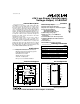
The MAX530 is a low-power, 12-bit, voltage-output digi-
tal-to-analog converter (DAC) that uses single +5V or
dual ±5V supplies. This device has an on-chip voltage
reference plus an output buffer amplifier. Operating cur-
rent is only 250µA from a single +5V supply, making it
ideal for portable and battery-powered applications. In
addition, the SSOP (Shrink-Small-Outline-Package) mea-
sures only 0.1 square inches, using less board area than
an 8-pin DIP. 12-bit resolution is achieved through laser
trimming of the DAC, op amp, and reference. No further
adjustments are necessary.
Internal gain-setting resistors can be used to define a
DAC output voltage range of 0V to +2.048V, 0V to
+4.096V, or ±2.048V. Four-quadrant multiplication is pos-
sible without the use of external resistors or op amps. The
parallel logic inputs are double buffered and are compati-
ble with 4-bit, 8-bit, and 16-bit microprocessors. For DACs
with similar features but with a serial data interface, refer
to the MAX531/MAX538/MAX539 data sheet.
________________________Applications
Battery-Powered Data-Conversion Products
Minimum Component-Count Analog Systems
Digital Offset/Gain Adjustment
Industrial Process Control
Arbitrary Function Generators
Automatic Test Equipment
Microprocessor-Controlled Calibration
____________________________Features
♦ Buffered Voltage Output
♦ Internal 2.048V Voltage Reference
♦ Operates from Single +5V or Dual ±5V Supplies
♦ Low Power Consumption:
250µA Operating Current
40µA Shutdown-Mode Current
♦ SSOP Package Saves Space
♦ Relative Accuracy: ±
1
/
2
LSB Max Over
Temperature
♦ Guaranteed Monotonic Over Temperature
♦ 4-Quadrant Multiplication with No External
Components
♦ Power-On Reset
♦ Double-Buffered Parallel Logic Inputs
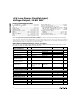
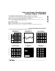
______________Ordering Information
Ordering Information continued on last page.
* Dice are tested at T
A
= +25°C, DC parameters only.
MAX530
+5V, Low-Power, Parallel-Input,
Voltage-Output, 12-Bit DAC
________________________________________________________________
Maxim Integrated Products
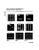
1
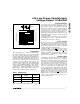
24
23
22
21
20
19
18
17
1
2
3
4
5
6
7
8
D0/D8
V
DD
ROFS
RFB
D4
D3/D11
D2/D10
D1/D9
TOP VIEW
VOUT
V
SS
REFOUT
REFGND
A0
D7
D6
D5
16
15
14
13
9
10
11
12
LDAC
CLR
AGND
REFIN
DGND
CS
WR
A1
DIP/SO/SSOP
MAX530
__________________Pin Configuration
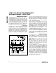
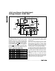
MAX530
REFOUT REFIN ROFS
2.048V
REFERENCE
POWER-ON
RESET
DAC LATCH
CONTROL
LOGIC
REFGND
AGND
CLR
A0
A1
CS
WR
LDAC
V
DD
DGND
V
SS
VOUT
RFB
17
14
NBL
INPUT
LATCH
D0/D8
D1/D9
D2/D10
D4
D3/D11
D6
D5
D7
NBM
INPUT
LATCH
NBH
INPUT
LATCH
24 1
234567
21
20
23
12
19
18 13 22
15
8
9
11
10
16
12-BIT DAC LATCH
________________Functional Diagram
Call toll free 1-800-998-8800 for free samples or literature.
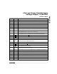
PART TEMP. RANGE PIN-PACKAGE
MAX530ACNG 0°C to +70°C 24 Narrow Plastic DIP
MAX530BCNG 0°C to +70°C 24 Narrow Plastic DIP
MAX530ACWG 0°C to +70°C 24 Wide SO
MAX530BCWG 0°C to +70°C 24 Wide SO
MAX530ACAG 0°C to +70°C 24 SSOP
MAX530BCAG 0°C to +70°C 24 SSOP
MAX530BC/D 0°C to +70°C Dice* ±1
±1
±
1
/
2
±1
±
1
/
2
±1
±
1
/
2
ERROR
(LSB)
19-0168; Rev 3; 7/95