
Datasheet
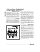
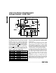

An additional 110µA of supply current can be saved
when the internal reference is not used by connecting
REFGND to V
DD
. A low on resistance N-channel FET,
such as the 2N7002, can be used to turn off the internal
reference to create a shutdown mode with minimum
current drain (Figure 3). When CLR is high, the transis-
tor pulls REFGND to AGND and the reference and DAC
operate normally. When CLR goes low, REFGND is
pulled up to V
DD
and the reference is shut down. At the
same time, CLR resets the DAC register to all 0s, and
the op-amp output goes to 0V for unity-gain and G = 2
modes. This reduces the total single-supply operating
current from 250µA (400µA max) to typically 40µA in
shutdown mode.
A small error voltage is added to the reference output
by the reference current flowing through the N-channel
pull-down transistor. The switch’s on resistance should
be less than 5Ω. A typical reference current of 100µA
would add 0.5mV to REFOUT. Since the reference cur-
rent and on resistance increase with temperature, the
overall temperature coefficient will degrade slightly.
As data is loaded into the DAC and the output moves
above GND, the op-amp quiescent current increases to
its nominal value and the total operating current aver-
ages 250µA. Using dual supplies (±5V), the op amp is
fully biased continuously, and the V
DD
supply current is
more constant at 250µA. The V
SS
current is typically
150µA.
The MAX530 logic inputs are compatible with TTL and
CMOS logic levels. However, to achieve the lowest
power dissipation, drive the digital inputs with rail-to-rail
CMOS logic. With TTL logic levels, the power require-
ment increases by a factor of approximately 2.
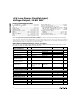
MAX530
+5V, Low-Power, Parallel-Input,
Voltage-Output, 12-Bit DAC
10 ______________________________________________________________________________________
MAX530
MAX530
12-BIT DAC LATCH
NBL
INPUT
LATCH
NBH
INPUT
LATCH
NBM
INPUT
LATCH
D0/D8
D1/D9
D2/D10
D4
D3/D11
D6
D5
D7
POWER-ON
RESET
CONTROL
LOGIC
DAC
A0
A1
CS
WR
LDAC
CLR
33µF
2.048V
REFERENCE
REFOUT REFIN ROFS
RFB
V
OUT
+5V
V
SS
DGND
2N7002
REFGND
AGND
V
DD
Figure 3. Low-Current Shutdown Mode
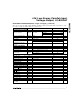
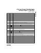
A0 A1 DATA UPDATED
L X X X X X Reset DAC Latches
H H X H X X No Operation
H X H H X X No Operation
H L L H H H NBH (D8-D11)
H L L H H L NBM (D4-D7)
H L L H L H NBL (D0-D3)
H H H L X X Update DAC Only
H L L X L L DAC NOT UPDATED
H L L L H H NBH and Update DAC
Table 2. Input Latch Addressing