
Datasheet


MAX530
+5V, Low-Power, Parallel-Input,
Voltage-Output, 12-Bit DAC
______________________________________________________________________________________ 11
V
IH
V
IL
DATA BITS
(8-BIT BYTE OR
4-BIT NIBBLE)
A0-A1
V
IL
V
IH
ADDRESS BUS VALID
t
AWH
t
CWS
t
WR
t
CWH
t
AWS
t
DS
t
DH
DATA BUS
VALID
NOTE: TIMING MEASUREMENT REFERENCE LEVEL IS
V
IH +
V
IL
2
t
CLR
CS
WR
CLR
LDAC
t
LDAC
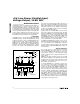
Figure 4. MAX530 Write-Cycle Timing Diagram
Parallel Logic Interface
Designed to interface with 4-bit, 8-bit, and 16-bit micro-
processors (µPs), the MAX530 uses 8 data pins and
double-buffered logic inputs to load data as 4 + 4 + 4
or 8 + 4. The 12-bit DAC latch is updated simultane-
ously through the control signal LDAC. Signals A0, A1,
WR, and CS select which input latches to update. The
12-bit data is broken down into nibbles (NB); NBL is
the enable signal for the lowest 4 bits, NBM is the
enable for the middle 4 bits, and NBH is the enable for
the highest and most significant 4 bits. Table 2 lists the
address decoding scheme.
Refer to Figure 4 for the MAX530 write-cycle timing
diagram.
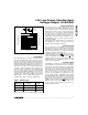
Figure 5 shows the circuit configuration for a 4-bit µP
application. Figure 6 shows the corresponding timing
sequence. The 4 low bits (D0-D3) are connected in paral-
lel to the other 4 bits (D4-D7) and then to the µP bus.
Address lines A0 and A1 enable the input data latches
for the high, middle, or low data nibbles. The µP sends
chip select (CS
) and write (WR) signals to latch in each of
three nibbles in three cycles when the data is valid.
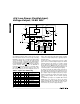
Figure 7 shows a typical interface to an 8-bit or a 16-bit
µP. Connect 8 data bits from the data bus to pins D0-D7
on the MAX530. With LDAC
held high, the user can load
NBH or NBL
+
NBM in any order. Figure 8a shows the
corresponding timing sequence. For fastest throughput,
use Figure 8b’s sequence. Address lines A0 and A1 are
tied together and the DAC is loaded in 2 cycles as 8 + 4.
In this scheme, with LDAC
held low, the DAC latch is
transparent. Always load NBL and NBM first, followed by
NBH.
LDAC
is asynchronous with respect to WR. If LDAC is
brought low before or at the same time WR
goes high,
LDAC
must remain low for at least 50ns to ensure the cor-
rect data is latched. Data is latched into DAC registers on
LDAC
’s rising edge.