
Datasheet


MAX530
+5V, Low-Power, Parallel-Input,
Voltage-Output, 12-Bit DAC
______________________________________________________________________________________ 15
33µF
REFIN
REFOUT
AGND
DGND
REFGND
ROFS
RFB
VOUT
V
OUT
-5V
+5V
MAX530
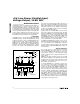
Figure 11. Bipolar Configuration (-2.048V to +2.048V Output)
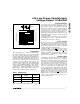
Figure 12. Four-Quadrant Multiplying Circuit
REFGND
AGND
DGND
REFIN
V
DD
V
SS
ROFS
RFB
VOUT
V
OUT
-5V
+5V
REFIN
MAX530
__________Applications Information
Single-Supply Linearity
As with any amplifier, the MAX530’s output op amp offset
can be positive or negative. When the offset is positive, it
is easily accounted for. However, when the offset is nega-
tive, the output cannot follow linearly when there is no
negative supply. In that case, the amplifier output (VOUT)
remains at ground until the DAC voltage is sufficient to
overcome the offset and the output becomes positive.
The resulting transfer function is shown in Figure 13.
Normally, linearity is measured after allowing for zero
error and gain error. Since, in single-supply operation,
the actual value of a negative offset is unknown, it can-
not be accounted for during test. In the MAX530, linear-
ity and gain error are measured from code 11 to code
4095 (see Note 2 under
Electrical Characteristics
). The
output amplifier offset does not affect monotonicity, and
these DACs are guaranteed monotonic starting with
code zero. In dual-supply operation, linearity and gain
error are measured from code 0 to 4095.
Power-Supply Bypassing
and Ground Management
Best system performance is obtained with printed cir-
cuit boards that use separate analog and digital ground
planes. Wire-wrap boards are not recommended. The
two ground planes should be connected together at the
low-impedance power-supply source.
AGND and REFGND should be connected together,
and then to DGND at the chip. For single-supply appli-
cations, connect V
SS
to AGND at the chip. The best
ground connection may be achieved by connecting
the AGND, REFGND, and DGND pins together and
connecting that point to the system analog ground
plane. If DGND is connected to the system digital
ground, digital noise may get through to the DAC’s ana-
log portion.
Bypass V
DD
(and V
SS
in dual-supply mode) with a
0.1µF ceramic capacitor connected between V
DD
and
AGND (and between V
SS
and AGND). Mount the
capacitors with short leads close to the device.
AC Considerations
Digital Feedthrough
High-speed data at any of the digital input pins may
couple through the DAC package and cause internal
stray capacitance to appear as noise at the DAC out-
put, even though LDAC and CS are held high (see
Typical Operating Characteristics
). This digital
feedthrough is tested by holding LDAC and CS high
and toggling the data inputs from all 1s to all 0s.
Analog Feedthrough
Because of internal stray capacitance, higher-frequen-
cy analog input signals at REFIN may couple to the
output, even when the input digital code is all 0s, as
shown in the
Typical Operating Characteristics
graph
Analog Feedthrough vs. Frequency. It is tested by set-
ting CLR to low (which sets the DAC latches to all 0s)
and sweeping REFIN.