
Datasheet
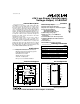
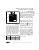

MAX530
+5V, Low-Power, Parallel-Input,
Voltage-Output, 12-Bit DAC
_______________________________________________________________________________________ 7
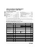
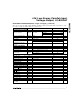
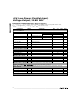
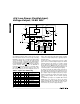
______________________________________________________________Pin Description
* This applies to 4 + 4 + 4 input loading mode. See Table 2 for 8 + 4 input loading mode.
D0 (LSB) Input Dta when A0 = 0 and A1 = 1, or D8 Input when A0 = A1= 1*
D0/D824
Positive Power Supply (+5V)V
DD
23
Offset Resistor Pin. Connect to VOUT for G = 1, to AGND for G = 2, or to REFIN for bipolar output.ROFS22
Feedback Pin. Op-amp feedback resistor. Always connect to VOUT.RFB21
Voltage Output. Op-amp buffered DAC output.VOUT20
Negative Power Supply. Usually ground for single-supply or -5V for dual-supply operation.V
SS
19
Reference Output. Output of the internal 2.048V reference. Tie to REFIN to drive the R-2R DAC.REFOUT18
Reference Ground must be connected to AGND when using the internal reference. Connect to V
DD
to disable the internal reference and save power.
REFGND17
Load DAC Input (active low). Driving this asynchronous input low transfers the contents of the input
latch to the DAC latch and updates VOUT.
LDAC16
Clear (active low). A low on CLR resets the DAC latches to all 0s.CLR15
Analog GroundAGND14
Reference Input. Input for the R-2R DAC. Connect an external reference to this pin or a jumper to
REFOUT (pin 18) to use the internal 2.048V reference.
REFIN13
Digital GroundDGND12
Chip Select (active low). Enables addressing and writing to this chip from common bus lines.CS11
Write Input (active low). Used with CSto load data into the input latch selected by A0 and A1.WR10
Address Line A1. Set A0 = A1 = 0 for NBL and NBM, A0 = 0 and A1 = 1 for NBL, A0 = 1 and
A1 = 0 for NBM, or A0 = A1 = 1 for NBH. See Table 2 for complete input latch addressing.
A19
Address Line A0. With A1, used to multiplex 4 of 12 data lines to load low (NBL), middle (NBM),
and high (NBH) 4-bit nibbles. (12 bits can also be loaded as 8+4.)
A08
D7 Input Dta, or tie to D3 and multiplex when A0 = 1 and A1 = 0*D77
D6 Input Dta, or tie to D2 and multiplex when A0 = 1 and A1 = 0*D66
D5 Input Dta, or tie to D1 and multiplex when A0 = 1 and A1 = 0*D55
D4
D3/D11
D2/D10
D1/ D9
NAME
D4 Input Dta, or tie to D0 and multiplex when A0 = 1 and A1 = 0*4
D3 Input Dta, when A0 = 0 and A1 = 1, or D11 (MSB) Input when A0 = A1 =1*3
D2 Input Dta, when A0 = 0 and A1 = 1, or D10 Input when A0 = A1 = 1*2
D1 Input Dta, when A0 = 0 and A1 = 1, or D9 Input when A0 = A1 = 1*1
FUNCTIONPIN