
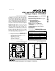
Datasheet

Output Buffer
The output amplifier uses a folded cascode input stage
and a type AB output stage. Large output devices with
low series resistance allow the output to swing to
ground in single-supply operation. The output buffer is
unity-gain stable. Input offset voltage and supply cur-
rent are laser trimmed. Settling time is 25µs to 0.01% of
final value. The output is short-circuit protected and
can drive a 2kΩ load with more than 100pF of load
capacitance. The op amp may be placed in unity-gain
(G = 1), in a gain of two (G = 2), or in a bipolar-output
mode by using the ROFS and RFB pins. These pins are
used to define a DAC output voltage range of 0V to
+2.048V, 0V to +4.096V or ±2.048V, by connecting
ROFS to VOUT, GND, or REFIN. RFB is always con-
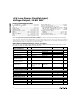
nected to VOUT. Table 1 summarizes ROFS usage.
External Reference
An external reference in the range (V
SS
+ 2V) to
(V
DD
- 2V) may be used with the MAX530 in dual-sup-
ply, unity-gain operation. In single-supply, unity-gain
operation, the reference must be positive and may not
exceed (V
DD
- 2V). The reference voltage determines
the DAC’s full-scale output. Because of the code-
dependent nature of reference input impedances, a
high-quality, low-output-impedance amplifier (such as
the MAX480 low-power, precision op amp) should be
used to drive REFIN.
If an upgrade to the internal reference is required, the
2.5V MAX873A is ideal: ±15mV initial accuracy,
7ppm/°C (max) temperature coefficient.
Power-On Reset
An internal power-on reset (POR) circuit forces the
DAC register to reset to all 0s when V
DD
is first applied.
The POR pulse is typically 1.3µs; however, it may take
2ms for the internal reference to charge its large filter
capacitor and settle to its trimmed value.
In addition to POR , a clear (CLR) pin, when held low,
sets the DAC register to all 0s. CLR operates asynchro-
nously and independently from chip select (CS). With
the DAC input at all 0s, the op-amp output is at zero for
unity-gain and G = 2 configurations, but it is at -V
REF
for the bipolar configuration.
Shutdown Mode
The MAX530 is designed for low power consumption.
Understanding the circuit allows power consumption
management for maximum efficiency. In single-supply
mode (V
DD
= +5V, V
SS
= GND) the initial supply cur-
rent is typically only 160µA, including the reference, op
amp, and DAC. This low current occurs when the
power-on reset circuit clears the DAC to all 0s and
forces the op-amp output to zero (unipolar mode only).
See the Supply Current vs. REFIN graph in the
Typical
Operating Characteristics
. Under this condition, there
is no internal load on the reference (DAC = 000hex,
REFIN is open circuit) and the op amp operates at its
minimum quiescent current. The CLR signal resets the
MAX530 to these same conditions and can be used to
control a power-saving mode when the DAC is not
being used by the system.
MAX530
+5V, Low-Power, Parallel-Input,
Voltage-Output, 12-Bit DAC
_______________________________________________________________________________________ 9
ROFS
CONNECTED TO:
DAC OUTPUT
RANGE
OP-AMP
GAIN
VOUT 0V to 2.048V G = 1
AGND 0V to 4.096V G = 2
REFIN -2.048V to +2.048V Bipolar
Note: Assumes RFB = VOUT and REFIN = REFOUT = 2.048V
Table 1. ROFS Usage
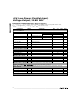
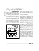
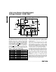
Figure 2. Reference Noise vs. Frequency
300
50
1 10 100
100
MAX531-FIG02
FREQUENCY (kHz)
REFERENCE NOISE (µV
RMS
)
150
200
250
0
0.1
1000
TOTAL
REFERERNCE
NOISE
R
S
REFOUT
C
REFOUT
C
S
TEK 7A22
C
REFOUT
= 3.3µF
C
REFOUT
= 47µF
SINGLE POLE ROLLOFF
1.8
1.6
1.4
1.2
1.0
0.8
0.6
0.4
0.2
0.0
REFERENCE NOISE (mVp-p)