
Datasheet


MAX5933A–MAX5933F/MAX5947A/B/C
Positive High-Voltage, Hot-Swap Controllers
10 ______________________________________________________________________________________
Applications Information
Hot-Circuit Insertion
When circuit boards are inserted into a live backplane,
the supply bypass capacitors on the boards draw high
peak currents from the backplane power bus as they
charge up. The transient currents can permanently
damage the connector pins and glitch the system sup-
ply, causing other boards in the system to reset.
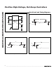
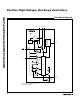
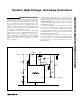
Power-Up Sequence
The power supply on a board is controlled by placing
an external n-channel MOSFET (Q1) in the power path
(Figure 5). Resistor R
SENSE
provides current detection
and capacitor C1 provides control of the GATE slew
rate. Resistor R6 provides current control-loop compen-
sation, while R5 prevents high-frequency oscillations in
Q1. Resistors R1 and R2 provide undervoltage sensing.
After the power pins first make contact, transistor Q1 is
turned off. When the voltage at ON exceeds the turn-on
threshold voltage, the voltage on V
CC
exceeds the
undervoltage lockout threshold, and when the voltage
on TIMER is less than 1.233V, transistor Q1 turns on
(Figure 6).
The voltage at GATE rises with a slope equal to
10µA/C1 and the supply inrush current is set at:
I
INRUSH
= C
L
x 10µA/C1
When the voltage across the current-sense resistor
R
SENSE
reaches V
SENSETRIP
, the inrush current is limit-
ed by the internal current-limit circuitry that adjusts the
voltage on GATE to maintain a constant voltage across
the sense resistor.
Once the voltage at the output has reached its final value,
as sensed by resistors R3 and R4, PWRGD goes high or
PWRGD goes low.
Short-Circuit Protection
The MAX5933_/MAX5947_ feature a programmable fold-
back current limit with an electronic circuit breaker that
protects against short circuits or excessive supply cur-
rents. The current limit is set by placing a sense resistor
between V
CC
(pin 8) and SENSE (pin 7).
To prevent excessive power dissipation in the pass
transistor and to prevent voltage spikes on the input
supply during short-circuit conditions at the output, the
current folds back as a function of the output voltage
that is sensed at FB (Figure 7).
When the voltage at FB is 0V, the current-limit circuit
drives GATE to force a constant 12mV drop across the
sense resistor. As the output voltage at FB increases,
the voltage across the sense resistor increases until FB
reaches 0.5V. At this point, the voltage across the
sense resistor is held constant at 47mV.
The maximum current limit is calculated as:
I
LIMIT
= 47mV / R
SENSE
For a 0.025Ω sense resistor, the current limit is set at
1.88A and folds back to 480mA when the output is
shorted to ground.
The MAX5933_/MAX5947_ also feature a variable over-
current response time. The time required to regulate
Q1’s drain current depends on:
1) Q1’s input capacitance
2) GATE capacitor C1 and compensation resistor R6
3) The internal delay from SENSE to GATE
Figure 8 shows the delay from a voltage step at SENSE
until GATE voltage starts falling, as a function of
overdrive.
POWER-UP WAVEFORMS
I
SENSE
2A/div
PWRGD
50V/div
OUTPUT
50V/div
GATE
50V/div
20ms/div
Figure 6. Power-Up Waveforms
V
CC
- V
SENSE
V
FB
12mV
47mV
0.5V0V
Figure 7. Current-Limit Sense Voltage vs. Feedback Voltage