
Datasheet


MAX5933A–MAX5933F/MAX5947A/B/C
Positive High-Voltage, Hot-Swap Controllers
______________________________________________________________________________________ 11
TIMER
TIMER provides a method for programming the maxi-
mum time the device is allowed to operate in current
limit. When the current-limit circuitry is not active,
TIMER is pulled to GND by a 3µA current source. After
the current-limit circuit becomes active, an 80µA pullup
current source is connected to TIMER, and the voltage
rises with a slope equal to 77µA/C
TIMER
, as long as the
current-limit circuit remains active. Once the desired
maximum current-limit time is chosen, the capacitor
value is:
C(nF) = 65 x t(ms)
or
T
LIMIT
= (C
TIMER
/80µA) x 1.233V
When the current-limit circuit turns off, TIMER is dis-
charged to GND by the 3µA current source.
Whenever TIMER reaches 1.233V, the internal fault
latch is set. GATE is immediately pulled to GND and
TIMER is pulled back to GND by the 3µA current
source. When TIMER falls below 0.5V, ON is pulsed low
to reset the internal fault latch.
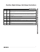
The waveform in Figure 9 shows how the output latches
off following a short circuit. The drop across the sense
resistor is held at 12mV as the timer ramps up. Since
the output did not rise, FB remains below 0.5V and the
circuit latches off. For Figure 9, C
T
= 100nF.
Undervoltage and Overvoltage Detection
ON can be used to detect an undervoltage condition at
the power-supply input. ON is internally connected to
an analog comparator with 80mV of hysteresis. If ON
falls below its threshold voltage (1.233V), GATE is
pulled low and is held low until ON is high again.
Figure 10 shows an overvoltage detection circuit. When
the input voltage exceeds the Zener diode’s breakdown
voltage, D1 turns on and starts to pull TIMER high. After
TIMER is pulled higher than 1.233V, the fault latch is set
and GATE is pulled to GND immediately, turning off
transistor Q1 (see Figure 11). Operation is restored
either by interrupting power or by pulsing ON low.
Power-Good Detection
The MAX5933_/MAX5947_ include a comparator for mon-
itoring the output voltage. The noninverting input (FB) is
compared against an internal 1.233V precision reference
and exhibits 80mV hysteresis. The comparator’s output
(PWRGD) is open drain and capable of operating from a
pullup as high as 80V. The PWRGD is similar to PWRGD
with an opposite polarity (active low) output.
The PWRGD (PWRGD) can be used to directly
enable/disable a power module with an active-high
enable input. Figure 12 shows how to use PWRGD to
control an active-low enable-input power module. Signal
inversion is accomplished by transistor Q2 and R7.
Supply Transient Protection
The MAX5933_/MAX5947_ are 100% tested and guar-
anteed to be safe from damage with supply voltages
up to 80V. However, spikes above 85V may damage
the device. During a short-circuit condition, the large
change in currents flowing through the power-supply
traces can cause inductive voltage spikes which could
exceed 85V. To minimize the spikes, the power-trace
parasitic inductance should be minimized by using
wider traces or heavier trace plating and a 0.1µF
bypass capacitor placed between V
CC
and GND. A
transient voltage suppressor (TVS) at the input can also
prevent damage from voltage surges.
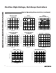
RESPONSE TIME TO OVERCURRENT
V
CC
- V
SENSE
(mV)
PROPAGATION DELAY (µs)
200100
2
4
6
8
10
12
14
0
0300
Figure 8. Response Time to Overcurrent
SHORT-CIRCUIT WAVEFORMS
I
SENSE
1A/div
TIMER
1V/div
OUTPUT
50V/div
GATE
50V/div
10ms/div
Figure 9. Short-Circuit Waveforms